This thread has been locked.

If you have a related question, please click the "Ask a related question" button in the top right corner. The newly created question will be automatically linked to this question.

TPS62122: Input impedance TPS6212

Part Number: TPS62122
Other Parts Discussed in Thread: TPS62120,

Hello , I am a French engineering student and for a project I am looking for the input impedance of the component TPS6212.

The idea is to represent the buck converter as a resistance for an ADS simulation.In order to do that I need the input impedance of the component.

I already submit a inqury, as a reply  the technical support indicates me an equation to find an input impedance of a Buck Converter at the bottom of page 3 of the following document : https://www.ti.com/lit/an/snva801/snva801.pdf?#page=3 

Now I will  see on LTSPICE or ADS if I can extract the input impedance of the circuit in Fig. 1 or 2. I would need to know what/how to define D in Matlab or ADS/LTSPICE ? 

Thanks in advance for your consideration,

Best,

Tom HENRY

  • Hi Tom,

    Matt will look into this and feedback to you soon.

    Thanks,

    Lishuang

  • Tom,

    The term "D" as used in the application note is the Duty Cycle  (D = Vout/Vin) of your converter design.

    Sincerely,

    -Matt

  • Hello Matt,

    Thanks for your reply,

    I have now 2 more interrogations :

    - What are the parametres for the circuit Fig 2 ( https://www.ti.com/lit/an/snva801/snva801.pdf?#page=3 in ordrer to implement it on LTSpice ?   

    - For the Equation 8 of the attached document Which parameters R,  L, C, D, s can be considered for the buck TPS62120  ? 

  • Tom,

    Technically none of these parameters are specific to the TPS62120 device itself.

    The L and C are the external Inductor and Capacitor, and as previously discussed the D represents the converter's duty cycle = Vout/Vin.

    For simplicity the inductor DCR and Capacitance ESR are ignored, and the same can be done for the internal FET RDSon, wich only leaves the DC load to be represented as "R".

    Sincerely,

    -Matt

  • Matt,

    We cannot properly model the internal circuit and take benefit from the equation provided in the datasheet, Can you please,  at least provide us an approximate value for the input impedance of that buck ? 

    Best,

    Tom

  • Tom,

    Can you please give me some more detail's on what it is you are trying to model?

    The application notes and details above were provided based on the assumption that you were looking for a small signal model of the Buck converter stage which is dominated by the external LC.

    Whereas, if you're just trying to model the power loss of the tps6212x device in your system, this would be need to be done in a different manner.

    Thank you,

    -Matt

  • Matt, 

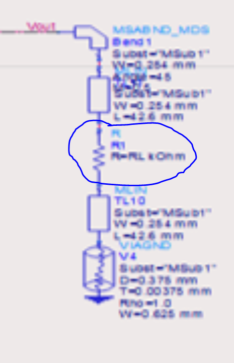
    The idea is to represent the buck TPS6212 as a resistance like this : 


    What I am looking for is Which value Can I take to represent the TPS6212 like this ?

  • Tom,

    I believe there was suppose to be an image attached to your previous post. 

    Can you please try re-posting with the image file for me to review?

    Thank you,

    -Matt

  • Matt,

    Sorry for the inconvenience, here is the image file :


    So the idea is to represent the buck converter as a resistance, the resistance value has to be equal to the input impedance of the component.

    Tom

  • Tom,

    My apologies, but it is still unclear to me what you are trying to do here?

    Is V4 your input voltage source, and is "Vout" the TPS62122  (Buck stage) output voltage?

    If so, as the the purpose of the power stage is to keep the output voltage fixed versus load, I'm failing to see how this model would be accurate.

    If you are merely trying to determine the power losses of the TPS62122 buck stage, as a first order these can be calculated based on the duty cycle of the converter (Vout/Vin), internal FET RDSon parameters, and Inductor DCR.

    Thank you,

    -Matt

  • Matt,

    It is a project on Energy Harvesting, the goal is to use RF ambient energy, convert it into DC signal with a Schottky diode and with the small DC signal ( Vout on the image file ) after the diode I want to use the TPS6212 to increase the DC current and power a microcontroller. For simulations I represent the Rload on the image file as the input impedance of the TPS6212.

    I hope it is more clear now

    Tom

  • Hi Tom,

    Matt will feedback to you tomorrow.

  • Tom,

    It seems to me that we are getting hung up on the terminology here, and it is not the input impedance of the TPS62122 device that you need for your model.  Instead, it sounds like you are trying to model the "effective load" that your Energy Harvesting output needs to support.

    To calculate this, you need to know what the TPS62122 output voltages and currents you are going to be.  (I expect these will be set by the microcontroller you are intending to use).

    Once the output voltage and current are established, as a first order you can use the efficiency curves in our datasheet to determine how much load would be reflected upstream based on the following equations:

    Pout = Vout*Iout (micro controller load)

    n = TPS62122 efficiency from datasheet

    Pin = Vin*Iin = Pout/n

    Iin = Pout / (n*Vin)

    Likewise, as P = V * I  & P = I^2 * R:

    Pin = Iin^2 * Rin = Pout/n

    Rin = Pout / (n*Iin^2)

    Ultimately, the efficiency curve in the datasheet are specific to the circuit we used to test out device.  In your design, the efficiency may vary based on the DCR of the inductor being used.

    Sincerely,

    -Matt