This thread has been locked.

If you have a related question, please click the "Ask a related question" button in the top right corner. The newly created question will be automatically linked to this question.

TPS61071-Q1: TPS61071 out ripple effect when input ripple

Part Number: TPS61071-Q1
Other Parts Discussed in Thread: TPS61071, TLV61046A

Hi team,

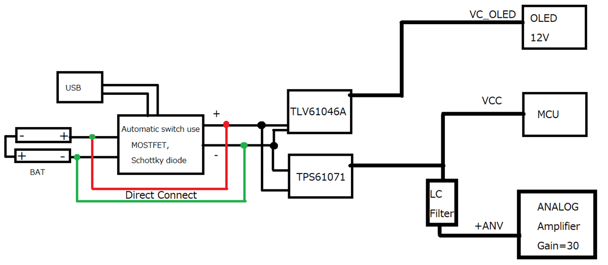
I am using TPS61071+TLV61046A for my project use two alkaline batteries in series boost to 3.3V for MCU and analog amplifier, boost to 12V for OLED.

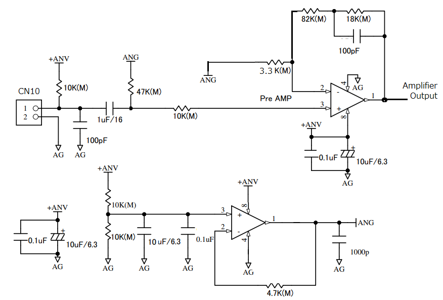
Connection diagram as shown below, When powering up (CN10 is OPEN)AmplifierOutput get low frequency noise(about 107Hz).Noise of AmplifierOutput is not exist when remove OLED. TPS61071 and TLV61046A of input and output I try increase the capacity of the electrolytic capacitor then the noise frequency will shift a little. If I connect battery direct to TPS61076 or TLV61046A or both noise of AmplifierOutput  is not exist. MOSTFET have RDS(on)=0.29ohm when VGS=2.5V. Please tell me what is issues ?How to resolve it?

Thanks and Best Regard

  • Hi Hanh:

    Please let me check at first. It's the same case for another post, right? 

  • Hi Minqiu,

    Yes, it is the same case for TLV61046A POST

    I understood and waiting.

    Best Regards

    Hanh

  • Hi Hanh:

    Got that. 

    As the load of the OLED is discrete, the input current will have large ripple without additional filter. So that I would recommend to add some filter is there is enough solution size. 

     If you only focus on the VCC power rail quality, you can add a filter after TPS61071. As the load is not so large at this power rail, the filter can use inductance in 0402 package.  

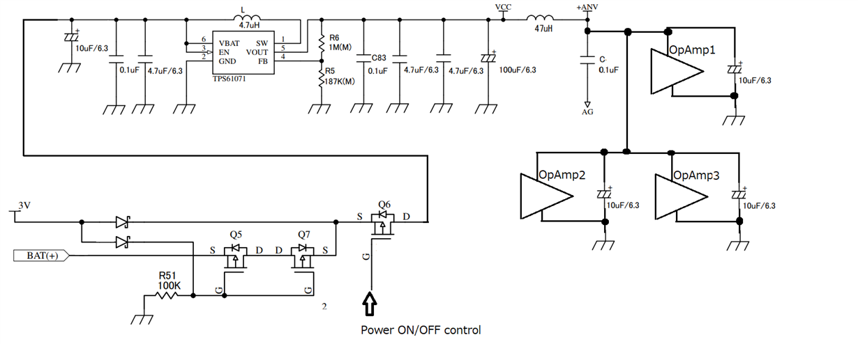
    In the other hand, I afraid the MOS bring additionally voltage drop. Could you share more details schematic including the MOS? And what's the voltage of the Battery? .................I afraid once there is a heavy load, the Vin drops lot, and the Rds of the MOS increase a lot with lower Vgs. It will make the result worse. 

  • Hi Minqiu,

    Thanks you very much!

    I also think the MOS bring additionally voltage drop.

    As show below I added LC filter after TPS61071 but noise is exist. Please tell me how to select the Value of L and C?This is low frequency noise ,LC filter can get it?

    If the OLED is off Battery current about 24mA.

    Thanks and Best Regards

    Hanh

  • Hi Hanh:

    For such connection, the BAT through three MOSFET to the Vbus. It added a lot of voltage drop. It's better to make the Vin strong and reliable. 

    According to the waveform "VCC", the frequency is not very low. So add a LC filter or 2-nd can do some help.  If you mean the audible noisy, soft-port capacitance and shield inductance may do some help

  • Hi Minqiu、

    Thanks for your reply.

    It is not audible noisy.

    The ripple of the output voltage of TPS61071 is small, but the current problem is that the input terminal of the amplifier circuit is pulled up to ANV, so even if the 2mV ripple of ANV is multiplied by 30, it becomes 60mv noise of the amplifier output. I tried other power supply ICs with good results (20mVp-pamplifier output noise), so I think the circuit design is bad, but the line response of TPS61071 is not very good. However, since it is currently in mass production, the TPS61071 cannot be changed. As an improvement, paralleling 820㎊ to R6 (1M) will reduce the noise a little. So I would like to add a higher capacitance ceramic capacitor, but is there any danger in adding a higher capacitance ceramic capacitor than 820pF?

    Best Regards

    Hanh

  • Hi Minqiu、

    As an improvement, parallelizing 10nF to R6 (1M) and the noise is reduced .Does adding a capacitor with a high than 10nF capacitance pose any danger to the TPS61071?

    Best Regards

    Hanh

  • Hi Hanh:

    Sorry for keeping you waiting. 

    I think you can do some load transient test to check if the loop is stable. And I don't think there is other risks. 

  • Hi Minqiu,

    Thanks for your reply

    I have just load transient test with LED blink (200ms ON/200ms OFF, Green led and current limit resistor is 220Ω)and get issue occurs

    with 2 PCB of 2 different PCB factories for different load response( gerber data is one) Vout of different ripple voltage 

    as show below pre amp noise output

    I don't understand what is the cause? I don't think the quality of the components(IC, resistor, ceramic capacitor.. etc). Is it possible due to the quality of PCB, via hole?

    Best Regard

    Hanh

  • Hi Hanh:

    Sorry that I missed  this post. Apology! 

    The layout is very important for a DCDC converter, and it's better to separate the power ground and signals. But it's hard for me to find out the root cause. 

    According to the waveform, it looks much better than previous. 

  • Hi Minqiu

    Thank for your reply.

    inductance down to 3.3uH and connecting parallel 47~100nF with R6(1M) my issue is resolved.

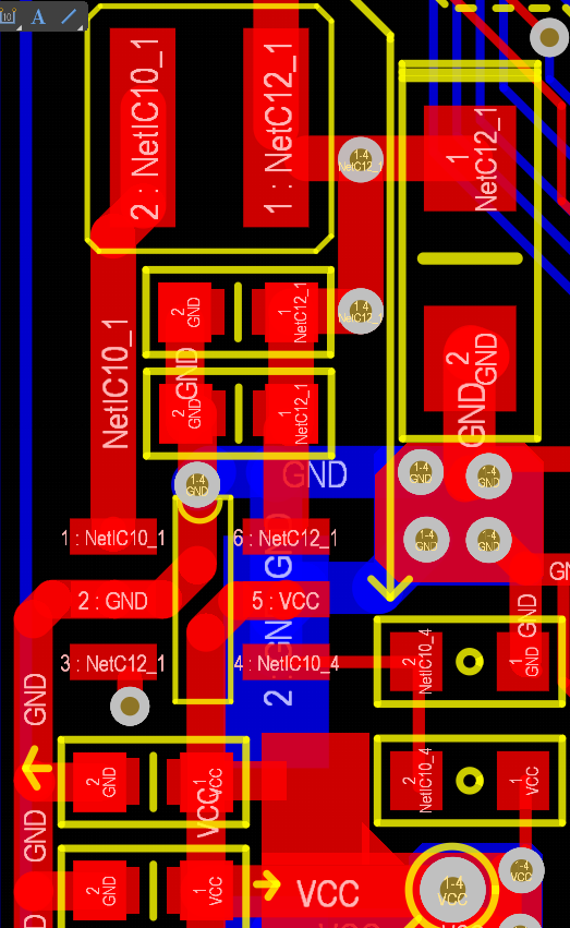
    I will also attach a TPS61071 pattern, so can you tell me if there are any bad points? 

    Unfortunately, in this time the pattern can not correction, but I will correct the pattern for the next production. 

    Thank you very much. 

    Best Regards!

  • Hello Hanh,

    Thank you very much for your feedback. It seems that you have been able to solve the issue. What do you mean with pattern?

  • Hi Minqiu,

     i am forget insert my PCB layout image, as show below any problem are there?

    Best regards!

    Hanh

  • Hello Hanh,

    For filtering the spikes that you observed on the last measurement, I would recommend to add a seperate ceramic cap on the supply pin of each OpAmp. Even if you do not populate it at the moment, having the ability to add a small cap there might be helpful.

    The converter should operate with the above layout, but I would recommend to work with GND layers instead of lines. A very simple estimation of voltage drop can be found here: 

  • Hi Brigitte,

    Thank you for your reply

    As show in image i am posted, The red pattern is layer 1, the blue pattern is layer 4, VCC plane is layer 2, GND plane is layer 3.

    i am added 0.1uF ceramic cap and 10uF tantalum cap on the supply pin of each OpAmp.

    Thank you for sending the reference link.

    Best Regards !

    Hanh