This thread has been locked.

If you have a related question, please click the "Ask a related question" button in the top right corner. The newly created question will be automatically linked to this question.

TPS53319: why the powergood signal of tps53319 is pull down

Part Number: TPS53319

hi sir

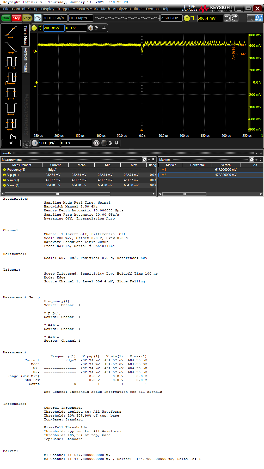
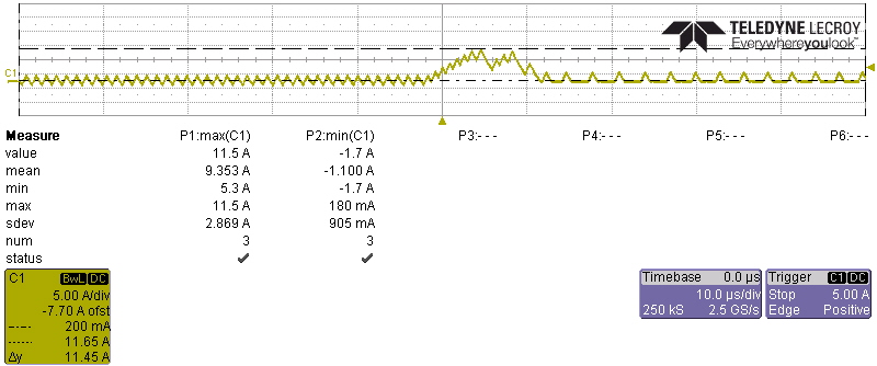
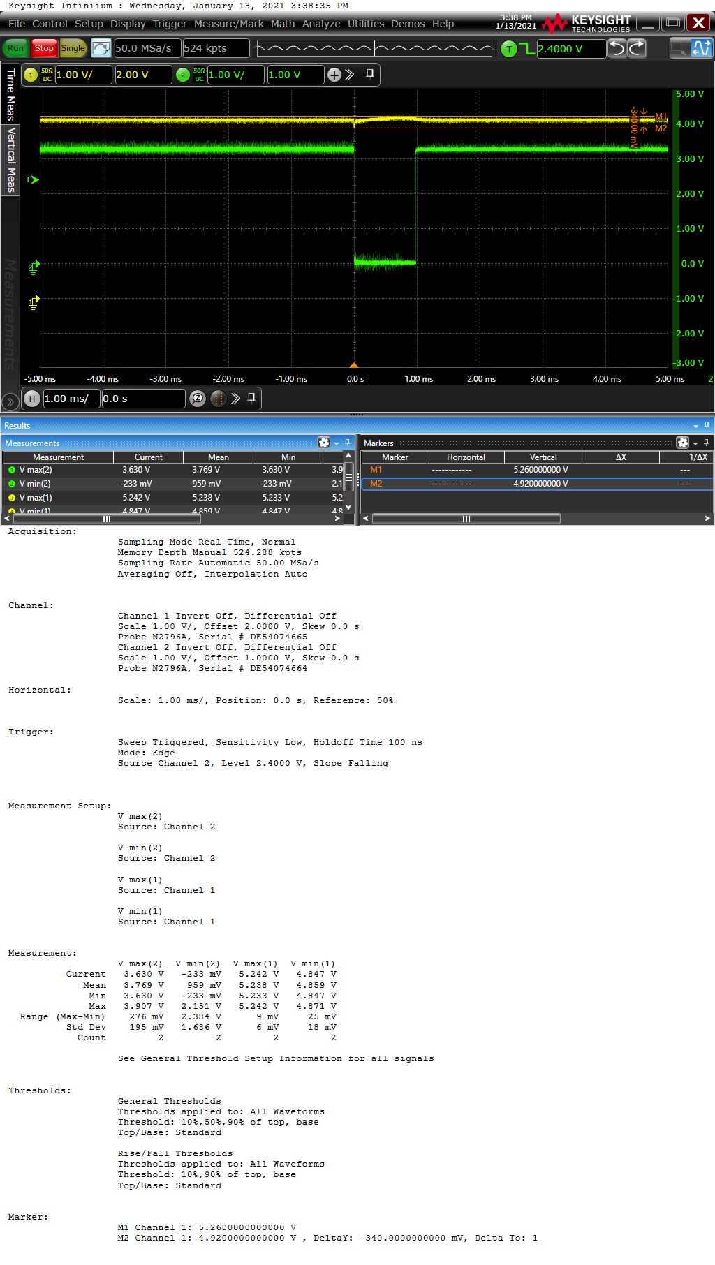
i'm using tps53319 to convert 12V downto 5V in my board,when the board is inserted a usb CD driver,the powergood signal of tps53319 is pull down a little while and then go high,i have measured the current and voltage of tps53319 when the USB CD driver is inserted,i don't think the current is high enough  and the voltage is low enough to pull PG down,the next 2 picture namly current and voltage, signal PG i have tested.

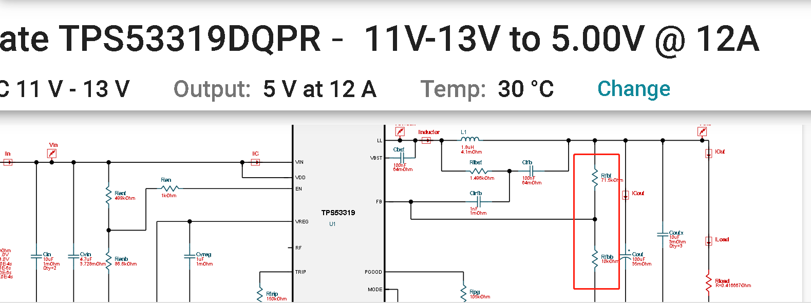
my design is next picture

Looking forward to your reply

  • Check the voltage on FB pin during the plug event?   I think FB pin voltage is drooping below the PGOOD threshold.

    The RCC circuit injects a ripple on to FB pin. 

    The dv/dt on output from the hot plug event may be coupling a transient onto the FB pin. 

    If the FB voltage is exceeding the PGOOD threshold, lower the values of R102, R100 and  R99 by 10x and increase R652 to 3k to minimize the ripple and coupling.

  • hi sir

    Thank you for you reply.

    I have measured the FB voltage,exactly,it have a glitch when the plug event. your suggestion of lower the values of
    R102, R100 and R99 by 10x and increase R652 to 3k solved the problem.
    Now i have some new questions

    1 What is The RCC circuit?
    2 the principle of the method to slove the problem.and I have tried lower the values of R102, R100 and R99 by
    5x,but it did not work.

    3Will it that lowering FB Voltage divider by 10x cause the loop stability?
    Looking forward to your reply

  • 1 What is The RCC circuit?

    The TPS53319 uses DCAP control and esr of the capacitor stabilizes the loop.  When using ceramic capacitor on output, the RCC is used to make the loop stable, by increasing voltageripple.  The RCC network is a circuit used to generate a triangular ramp that is in phase with the inductor current. This triangular ramp is then AC-coupled into the feedback node. 


    2 the principle of the method to slove the problem.and I have tried lower the values of R102, R100 and R99 by
    5x,but it did not work.

    I suspect the dV on the output capacitor, causes the capacitors in the RCC network to inject current (i=c*dV/dt) into the FB node.   The FB pin is high impedance and  the fb voltage offset is created with the 10k and ~70k feedback resistors and dV injected current.  Lowering the values of the feedback resistors lowers the offset. 

    The R652 change to 3k, reduces the injection voltage. 

    I think the summation of the RCC ripple injection and the dV induced injections causes the FB pin voltage to deviate by -5%, causing the PGOOD pin to assert.

    3Will it that lowering FB Voltage divider by 10x cause the loop stability?

    It can, but in your in your case no.   The 10x lower divider will

    use more current and will be less sensitive to noise.   

    the following app note has equation 4 for stability and feedback resistors. 

      www.ti.com/.../slva453.pdf   

  • hi sir

    Thanks for your reply.

    I seem to understand.

    Dose RCC  circuit in my schematic diagram is consist  of  R652, C996,C207?

    another question is why  the voltage of FB pin has a glitch but the output dose not have a glitch since they are connect by pure resistance circuit (r98,r99,r100) each other?

  • Dose RCC  circuit in my schematic diagram is consist  of  R652, C996,C207?

    Yes, R652, C996 and C207 is the RCC injection circit 

    another question is why  the voltage of FB pin has a glitch but the output dose not have a glitch since they are connect by pure resistance circuit (r98,r99,r100) each other?

    I am not sure I understand the question,   the yellow waveform in oscope plot above has a glitch from the load connecting and PGOOD pins responds. 

    The RCC injects a ripple voltage which is small on the FB pin.  The FB pin is high impedance, the vout node is low impedance, so the small ripple from the RCC would be difficult to differentiate from the typical ripple voltage on the output.   A output voltage drooping from a load step on the output would be noticeable on the FB.   

  • hi sir 

    Thanks for your reply.

    I have read the document named slva453 about derivation formula of VFB, but I didn't find the voltage of FB pin influenced by the feedback resistors R102, R100 and R99.it relates to current ripple,frequence of switch and out of capacitance. So,how  to understand Your previous explanation about "fb voltage offset is created with the 10k and ~70k feedback resistors and dV injected current. Lowering the values of the feedback resistors lowers the offset. "

    Looking forward to your reply.

  • The SLVA453 document is discussing the steady state operation of the RCC circuit. 

    Equation 9 discusses the Vinj and the offset created from the ripple in the steady state operation. 

    The hypothesis is that you have an issue of the PGOOD pin asserting because of the load step transient on the

    output causing the FB pin voltage to cross the PGOOD threshold. 

    The change in output voltage (ie.  dVo/dt)  on the  capacitors in the RCC circuit inject current into the FB pin (Ifb).

    Ifb = C * dVo/dt.         

    The FB pin is high impedance, so the current flows through the FB resistors.    Ifb * Rfb = dVfb       Larger resistance causes larger voltage.

         Rfb = 10k // 70k      =  8 - 9kOhm         if you use 1k and 7k   the equivalent resistance is 875 ohms. 

    I believe the output voltage transient is causing a transient voltage on the FB pin and lowering the FB resistors reduces the offset, changing the C values in the RCC is not good option since stability can be affected.          

  • hi sir 

    The problem has solved,I agree with your judgment on this issue.

    But I have some new questions.

    I have read the datasheet of TPS53319,it recommends the feedback resistors are 10k+

    and I use TI  WEBENCH POWER DESIGNER to design buck circuit,it‘s’ recommendation  of  feedback resistors also  are 10k+

    Why are recommended designs all requires the feedback resistor of R2 is 10K+ ? 


    Is this TI's standard design?

    Dose this scheme can't solve the problem that Instantaneous current is large,so we must lower the R2 10x to solve the problem of large instantaneous current?

    lower the R2 10x can solve the problem of large instantaneous current,Will this cause other problems?since the current design and reference design are different in the feedback resistance

    I may need to rework hundreds of devices. I'm worried that rework will lead to other unpredictable problems

    Looking forward to your reply

  • The 10kOhm to 20kOhm is a guideline to bound the resistor selection and

    minimize problems is an extreme high or low value is used. 

    When using 10k the power dissipation is low, there is low offset

    from leakage current and the noise immunity is good. 

    Using a 1000kOhm on feedback could have noise issues on some board layouts

    and the leakage currents may cause an output voltage error. 

    Using a 1kOhm, the current draw is greater than the 10kOhm. 

    I do not see lowering the resistors values causing an issue.  The resistor is setting a dc gain.   

    The efficiency can be lower if operating in the Skip mode with low value feedback resistors. 

    In your application, lowering the feedback resistors minimizes the output offset from the RCC circuit. 

    If you raised your feedback resistor values, we would possibly adjust the R value in the RCC circuit to minimize the offset.

    I am assuming the change in vout during transient is acceptable and meets spec. 

    If not, consider adding or changing Cout to minimize droop. 

    During your tests, Do you have 18 x 10uF/6.3V ceramics capacitor and a 330uF on output?    If so, what is the ESR of the 330uF?

    From the oscope plot, the vout droop is causing the PGOOD to go low.  Correct?   Another method to minimize vout droop, is to add Cout or use lower esr Cout capacitors.   

    The 330uF is electrolytic and will have esr.  The 10uF ceramics are low esr.   Since the output voltage is 5V and the ceramics are rated for 6.3V, the effective capacitance for a 10uF could be between 2uF to 6uF depending in package size.   Using some 22uF/6.3V or 10uF/10V caps may help load step response.      

    The ROVP can cause the PGOOD pin to go low when the output voltage is OV.   I would set the threshold with a different resistor network to reduce the possiblity of the triggering ROVP to low.     As a troubleshooting test,   set R674 to 0 ohms, when testing the load step.    I do not think ROVP is causing the current issue, but wanted to highlight a possible issue. 

  • hi sir

     Thanks for your reply.

    1 If you raised your feedback resistor values, we would possibly adjust the R value in the RCC circuit to minimize the offset.

    Is that means  in my application do not change the value of the feedback resistors but changes the R value of RCC can solve my trouble ?

    But I adjust the R value in the RCC from 100 to 10K,the problem has not been solved.

    2  If not, consider adding or changing Cout to minimize droop. During your tests, Do you have 18 x 10uF/6.3V ceramics capacitor and a 330uF on output?    If so, what is the ESR of the 330uF?

    Yes Cout has  18 x 10uF/6.3V ceramics capacitor and a 330uF on output. and I have added anohter 330uF capacitor, but the problem has not been solved.ESR of  330uF is 170 mohm.

    3 From the oscope plot, the vout droop is causing the PGOOD to go low.  Correct?   Another method to minimize vout droop, is to add Cout or use lower esr Cout capacitors.  

    I think  vout droop don't  cause PGOOD to go low,As you guessed before the VFB may be the cause of PG pull down.the next  oscope plot is vfb when usb device is plugged.


  •  Thanks for your reply.

    1 If you raised your feedback resistor values, we would possibly adjust the R value in the RCC circuit to minimize the offset.

    Is that means  in my application do not change the value of the feedback resistors but changes the R value of RCC can solve my trouble ?

    But I adjust the R value in the RCC from 100 to 10K,the problem has not been solved.

    DD) No, raising the R in the RCC does not resolve the issue, it is a response to the 10k to 20k constraint.  the offset is DC offset from the ripple voltage and the feedback resistors.  the issue we are observing is ac coupling of the vout drooping and injected into the FB pin. 

    2  If not, consider adding or changing Cout to minimize droop. During your tests, Do you have 18 x 10uF/6.3V ceramics capacitor and a 330uF on output?    If so, what is the ESR of the 330uF?

    Yes Cout has  18 x 10uF/6.3V ceramics capacitor and a 330uF on output. and I have added anohter 330uF capacitor, but the problem has not been solved.ESR of  330uF is 170 mohm.

    DD) The esr of 170mOhm is very high.   A 330uF with an esr <30mohm would minimize the voltage droop during the load transient.   If the vout voltage droop does not meet spec consider changing capacitor or increasing value of ceramic capacitors. 

    3 From the oscope plot, the vout droop is causing the PGOOD to go low.  Correct?   Another method to minimize vout droop, is to add Cout or use lower esr Cout capacitors.  

    I think  vout droop don't  cause PGOOD to go low,As you guessed before the VFB may be the cause of PG pull down.the next  oscope plot is vfb when usb device is plugged.

    DD) In summary, use the 10x lower feedback resistors to reduce FB transient during load plug event to resolve PGOOD assertion.    Consider using a lower esr 330uF (>30mOhm) to minimize voltage droop