A related question is a question created from another question. When the related question is created, it will be automatically linked to the original question.
If you have a related question, please click the "Ask a related question" button in the top right corner. The newly created question will be automatically linked to this question.
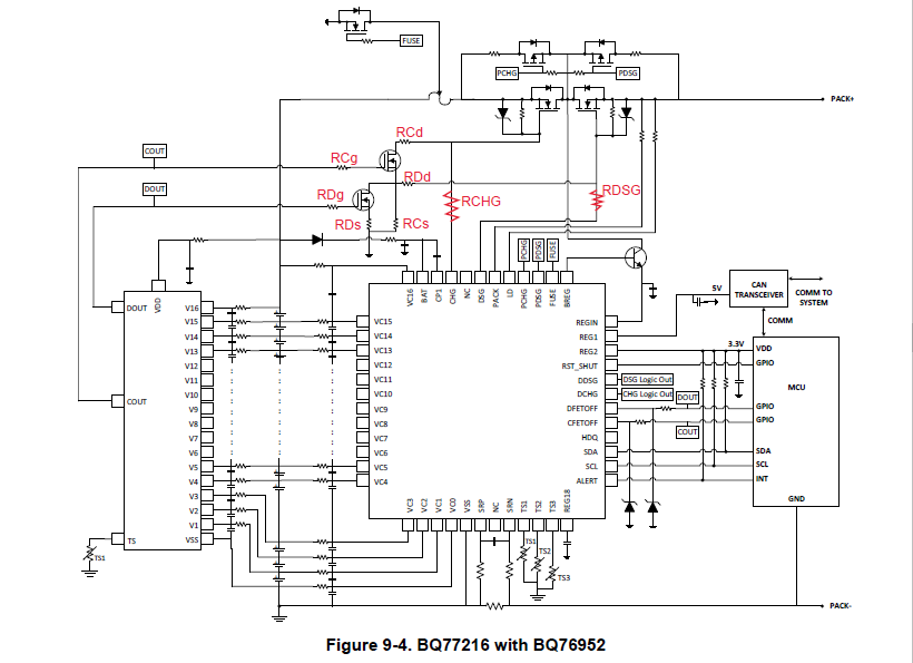
BQ77216: Parameter consult of BQ77216 for BQ76952 secondary protection
Part Number: BQ77216 Other Parts Discussed in Thread: BQ76952,
Hi Expert,
I have noticed that we have recommended circuit, that BQ77216 work with BQ76952. My questions is how to select gate resistor as following fig shows. Thanks!
The figure did not come through the posting, but I expect you are referring to figure 9-4 of the BQ77216 data sheet. The figure 9-4 shows resistors in the gate, source and drain path of an N-channel signal FET to pull down the gate drive from the BQ76952. The BQ76952 data sheet does not specify a maximum charge pump current which it can provide, but from the start up time with a constant current assumption 100 ms and 11V into 470 nF (I = C x dV/dt) would give 51.7 uA. You would want to provide at least as much current as the BQ76952 can produce with a comfortable margin since there is no specification. You likely don't want too small of a resistor value since for the charge FET it will load the battery through the gate-source Zener. Consider power dissipation in the resistor as well.
For discharge the resistor can be smaller since the discharge FET will turn off. With the charge pump current limited it will draw extra current as indicated in the shorted charge pump condition in the note in table 16-3 of the data sheet.
For the N-channel signal FET resistors:
The gate resistor will control switching speed.
The source resistor could limit the current drawn with the VGS level of the FET, but a maximum output voltage is not specified for CO and DO.
The drain resistor will limit current drawn from the battery and BQ76952 charge pins for the charge connection, and from the load for the discharge connection.
I will propose 20k for gate resistor(6V/0.3mA = 20k). For CHG/DSG pull down resistor, I will propose 500k (85V/51.7uA = 1.6M). Will give you some feedback when customer power on thier system. Thanks!
I get confused so I will add a marked picture from figure 9-4 of the BQ77216 data sheet.
The BQ77216 data sheet does not give a typical or maximum voltage of VOUT_AH, it shows 0 to 1.5V below the supply with a minimum of 6V when regulated. So the RDs and RCs could be 0 or select a value appropriate for the signal FETs chosen.
If using the CFETOFF and DFETOFF signals into the BQ76952 you will need to limit the voltage into the pins, pick a resistor suitable for the zeners used, and check the input current. I would expect a few k to 20k would be ok.
The RCg and RDg can be chosen for turn on speed of the signal FETs, again I would expect a few k to 20k ohm.
The RDSG and RCHG would come from the BQ76952 design for switching speed.
The RCd and RDd will pull down the FET gates. They must overcome the charge pump current if the BQ76952 is leaving them on, you may want them to mimic the turn off speed from the BQ76952. They will also pull against the battery or the PACK voltage when on. Because of the swing of the FET gates is different, the resistors might be different. If the BQ76952 RCHG resistor is 5.1k ohm, it will turn off initially with a 11V/5.1k =~ 2.2 mA current. If the battery operates from 50 to 65 V, at 76 V a 33 k ohm resistor would give about 2.3 mA. With the battery at low voltage of 50V the resistor would still be drawing about 1.5 mA from the charge FET gate-source zener and the CHG pin of the BQ76952. Consider the power in the resistor. The discharge FET may have a higher turn off current, but the gate will transition to GND when off, so the power should be lower, so the resistor may be smaller. Consider though that the resistor will be discharging the PACK capacitance through the zener on the discharge FET gate to source Zener.