This thread has been locked.

If you have a related question, please click the "Ask a related question" button in the top right corner. The newly created question will be automatically linked to this question.

TPS650864: Inquiry about TPS6508640 design

Guru 10890 points
Part Number: TPS650864
Other Parts Discussed in Thread: TPS650861

Hello,

My customer is reviewing the design of the TPS6508640 to power the ZU15EG as shown below.

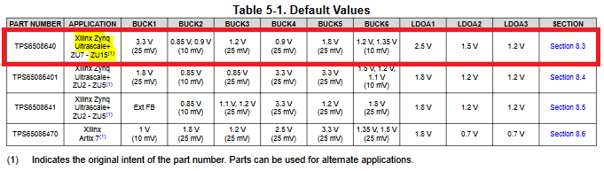
The customer should use 3.3V as the VCCO_HDIO, but the max output voltage of the LDOA2 is 1.5V.

So, They want to connect the LDOA2 1.5V output to the enable pin of an external LDO device suppling 3.3V to the VCCO_HDIO.

Also, to increase effciency, they want to connect an external 5V to BUCK 3/4/5 input and an external 3.6V to the SWA1 input without using the cascade connection BUCK1.

The external 5V and 3.6V are the first inputs because the customer uses Vin 5V application.

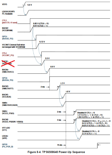
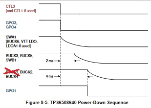
Please advise if this configuration has no problems with the power up/down sequence operation below except for BUCK1.

Thank you.

JH

  • Hello JH,

    I do not see any issue with that approach, though I have three comments:

    • LDOA2 won't turn on by default, so just clarifying that if they are using it to enable an external LDO, it would need to be controlled by I2C
      • Otherwise if they want it somewhere else in the sequence, they would need to use a rail in the sequence
    • BUCK1 will be turned on in this OTP memory, so even if they aren't using it, the power fault monitoring will be active
      • If they are planning to use it, then no issue
      • If they are not planning to use it, then FBVOUT1 will still need a 3.3V supply to avoid power faulting. This can come from a resistor divider from 5V instead of FETs + inductor, though I will note that there should be a small capacitor (>1 nF) from FBVOUT1 to GND to stabilize the FBVOUT1 pin.
    • SWA1 has power fault monitoring masked, so no issue with 3.6V input there for TPS6508640

    My last comment would be that if they find they want to continue making more changes, TPS650861 is the user programmable version of TPS6508640 that would allow changes to the default OTP settings. These can be programmed by the user during the production or bought pre-programmed with their specific settings from Arrow. It sounds like so far they may be OK with existing settings but just providing this as an option.

  • Hi Kevin,

    Thank you for your reply.

    The customer wants to use the TPS6508640 without I2C control. And to reduce the size, they want to remove the unused BUCK1's inductor and FET.

          1. If the user don't use LDOA2/3,  is it okay to not use I2C contol?

              The user thinks that Figure 8-4 TPS6508640 Power-Up Sequence is performed only with OTP setting and circuit connection without I2C control. Is this right?

          2. If the user supplies 3.3V to FBVOUT1 pin, is it okay to remove the inductor and FET from BUCK1?

    Thank you.

    JH

  • Hello JH,

    1. Correct - I2C is not needed as long as they don't use any of the rails that are not part of Figure 8-4.

    2. Correct, though I have made an FAQ about this - it is recommended to also add a capacitor if a resistor divider is used: e2e.ti.com/.../971278

  • Hello Kevin,

    Thank you for your help.

    Could you please tell us how SWB2 will work? Is control by I2C necessary to turn on SWB2?

    We could not find SWB2 in the Figure 8-4 TPS6508640 Power-Up Sequence.

    Thank you.

    JH

  • Hi JH,

    You are correct, SWB2 is not used in this OTP. If it is needed, then it would need to be enabled by I2C.