This thread has been locked.

If you have a related question, please click the "Ask a related question" button in the top right corner. The newly created question will be automatically linked to this question.

UCC2813-0: Webench design transformer spice model

Part Number: UCC2813-0
Other Parts Discussed in Thread: UCC28C40-Q1, UCC28C40

Webench created a schematic with a transformer. We would like to simulate the design with TINA spice 12, but need help setting up the transformer for the simulation.

  • David,

    Thanks for your interest in TI here. What sort of simulation are you trying to run and what are you hoping to learn from it? Are you trying to verify the selection of transformer parameters for the design?

    Please share your webench design information as well so we better understand your specifications.

    Regards,

    John

  • Here is the output from Webench:

    How do you create the transformer in Tina for the following?

  • I just got back in to see if there were any comments added and noticed that schematic I cut and pasted is not showing up. I'm trying again by converting the Webench output to a Word document.


    WEBENCH ®     Design Report

    Design : 14 UCC2813DTR-0

    UCC2813DTR-0 10V-264V to 12.00V @ 1A


    VinMin = 10.0V VinMax = 264.0V Vout = 12.0V Iout = 1.0A


    Device = UCC2813DTR-0

    Topology = Flyback

    Created = 2021-01-13 14:52:35.171 BOM Cost = NA

    BOM Count = 45 Total Pd =


    Dsec2

    VF@Io= 500.0 m V

    VRRM= 666.977 V


    T1

    Dsec

    VF@Io= 500.0 m V

    VRRM= 666.977 V


         Vin


    Cin

    2.2 µF

    14.0 m Ohm


    Rstartup1

    4.7 kOhm

    250.0 m W


    Rsnub2

    1.2 kOhm

    2.0 W


    Rsnub1

    1.2 kOhm

    2.0 W


    Csnub                                                     

    180.0 nF                                        

    1.0 m Ohm

    Dsnub

    VF@Io= 1.0 V

    VRRM= 400.0 V


    Cout 1

    180.0 µF

    16.0 m Ohm


    Iout


    Cref

    100.0 nF

    1.0 m Ohm


    UCC2813 - 0 D


    Rstartup2

    4.7 kOhm

    250.0 m W


    C12

    100.0 nF

    64.0 m Ohm


    Cvcc

    33.0 µF

    700.0 m Ohm


    Raux

    10.0 Ohm

    63.0 m W


    Daux

    VF@Io= 500.0 m V

    VRRM= 503.488 V


    Rz

    1.1 kOhm

    63.0 m W


    Q1


    Rfbt


    Ct

    1.0 nF

    25.0 m Ohm


    Qsc


    C13

    1.0 nF


    REF


    RC

    FB U1 COMP CS


    VCC


    OUT


    GND


    Rdrv

    12.1 Ohm

    63.0 m W


    M1

    VdsMax= 356.0 V IdsMax= 6.0 Amps


    13.7 kOhm

    63.0 m W


    Dz


    Rt

    15.4 kOhm

    50.0 m W


    Rsc

    3.24 kOhm

    63.0 m W


    R11

    10.0 kOhm

    50.0 m W


    Ccs

    470.0 pF


    Rcs

    1000.0 Ohm

    63.0 m W


    Rsns

    167.617 m Ohm

    0.0 W


    Rled

    1.21 kOhm

    63.0 m W


    Rbias

    4.87 kOhm

    63.0 m W


    R21

    10.0 kOhm

    50.0 m W


    D21

    VF@Io= 550.0 m V

    VRRM= 30.0 V


    C21

    22.0 µF

    2.05 m Ohm


    C22

    22.0 pF


    R13

    4.99 kOhm

    63.0 m W


    O1                                                                                                                                    R22

    2.49 MOhm

    63.0 m W


    C23

    1.23429 pF


    R12

    1.43 kOhm

    63.0 m W


    VR


    Rfbb

    3.6 kOhm

    100.0 m W


    Design Alerts


    Component Selection Information

    Click on the transformer symbol in the schematic and select "Explore Transformer Core/Bobbin Selection" to design using specific transformer cores and bobbin. With the current design condition, suitable FET could not be found in the current database. Hence, this design is created using an ideal FET. Please note that the resulting FET parameters are ideal, so the efficiency/loss values have been disabled. Also, the schematic/PCB export and Thermal simulations will not work with the ideal FET.


    Electrical BOM


    Name


    Manufacturer


    Part Number


    Properties


    Qty

    Price

    Footprint

    C12


    Kemet


    C0805C104M5RACTU


    Cap= 100.0 nF


    1

    $0.01


    Series= X7R


    ESR= 64.0 mOhm

    VDC= 50.0 V


    0805 7 mm2


    IRMS= 1.64 A


    C13


    MuRata


    GRM1555C1H102JA01J


    Cap= 1.0 nF


    1

    $0.01


    Series= C0G/NP0


    VDC= 50.0 V

    IRMS= 0.0 A


    0402 3 mm2

    C21


    TDK


    C2012X5R1V226M125AC


    Cap= 22.0 uF


    1

    $0.33


    Series= X5R


    ESR= 2.05 mOhm

    VDC= 35.0 V


    0805 7 mm2


    IRMS= 4.5559 A


    C22


    Samsung Electro-


    CL21C220JBANNNC


    Cap= 22.0 pF


    1

    $0.01


    Mechanics


    Series= C0G/NP0


    VDC= 50.0 V

    IRMS= 0.0 A


    0805 7 mm2

    C23


    CUSTOM


    CUSTOM


    Cap= 1.23429 pF


    1

    NA


    Series= ?


    VDC= 0.0 V

    IRMS= 0.0 A


    CUSTOM 0 mm2

    Ccs


    AVX


    04025A471JAT2A


    Cap= 470.0 pF


    1

    $0.01


    Series= C0G/NP0


    VDC= 50.0 V

    IRMS= 0.0 A


    0402 3 mm2


    Name         Manufacturer                     Part Number                                   Properties                      Qty Price       Footprint

    Cin             TDK                                   B32674D4225K

    Series= B32674


    Cap= 2.2 uF

    ESR= 14.0 mOhm

    VDC= 450.0 V

    IRMS= 6.0 A


    1       $0.94


    CAPRR2750W80L3150T1250H2150

    486 mm2

    Cout1         Panasonic                         25SVPF180M Series= SVPF


    Cref            MuRata                              GRM155R71C104KA88D

    Series= X7R


    Csnub        MuRata                              GRM188R71E184KA88D

    Series= X7R


    Ct               Kemet                                 C0805C102J1GACTU

    Series= C0G/NP0


    Cvcc          Panasonic                         EEE-FK1E330UR Series= FK


    Cap= 180.0 uF

    ESR= 16.0 mOhm

    VDC= 25.0 V

    IRMS= 4.65 A


    Cap= 100.0 nF

    ESR= 1.0 mOhm

    VDC= 16.0 V

    IRMS= 0.0 A

    Cap= 180.0 nF

    ESR= 1.0 mOhm

    VDC= 25.0 V

    IRMS= 0.0 A

    Cap= 1.0 nF

    ESR= 25.0 mOhm

    VDC= 100.0 V

    IRMS= 1.71 A

    Cap= 33.0 uF

    ESR= 700.0 mOhm

    VDC= 25.0 V

    IRMS= 160.0 mA


    1       $0.63


    1       $0.01


    1       $0.03


    1       $0.09


    1       $0.09


    CAPSMT_62_E12 106 mm2


    0402 3 mm2


    0603 5 mm2


    0805 7 mm2


    SM_RADIAL_C 62 mm2

    D21            Panasonic                         DB2S31600L                                  VF@Io= 550.0 mV VRRM= 30.0 V

    Daux          CUSTOM                              CUSTOM                                          VF@Io= 500.0 mV VRRM= 503.488 V

    Dsec          CUSTOM                              CUSTOM                                          VF@Io= 500.0 mV VRRM= 666.977 V

    Dsec2        CUSTOM                           CUSTOM                                       VF@Io= 500.0 mV VRRM= 666.977 V

    Dsnub        SMC Diode Solutions        UF4004TA                                      VF@Io= 1.0 V VRRM= 400.0 V


    1       $0.03


    1       NA


    1       NA


    1       NA


    1       $0.22


    SOD-523 5 mm2


    CUSTOM 0 mm2


    CUSTOM 0 mm2


    CUSTOM 0 mm2


    DO-41 43 mm2

    Dz               ON Semiconductor            MMBZ5239BLT1G                         Zener                             1       $0.02


    M1              NA                                      IdealFET                                           VdsMax= 356.0 V IdsMax= 6.0 Amps


    1       NA


    SOT-23 14 mm2


    NA 0 mm2

    O1              Fairchild Semiconductor    FOD817A                                       Optocoupler                   1       $0.11


    Q1              Diodes Inc.                        MMBT4401-7-F                              Bipolar Transistor          1       $0.02


    DIP-4 71 mm2


    Qsc            STMicroelectronics            2N2222A                                        Bipolar Transistor          1       $1.11


    SOT-23 14 mm2


    R11            Yageo                                RC0201FR-0710KL

    Series= ?


    R12            Vishay-Dale                       CRCW04021K43FKED

    Series= CRCW..e3


    R13            Vishay-Dale                       CRCW04024K99FKED

    Series= CRCW..e3


    Res= 10.0 kOhm

    Power= 50.0 mW

    Tolerance= 1.0%

    Res= 1.43 kOhm

    Power= 63.0 mW

    Tolerance= 1.0%

    Res= 4.99 kOhm

    Power= 63.0 mW

    Tolerance= 1.0%


    1       $0.01


    1       $0.01


    1       $0.01


    TO-18 57 mm2


    0201 2 mm2


    0402 3 mm2


    0402 3 mm2


    Name         Manufacturer                     Part Number                                   Properties                      Qty Price       Footprint

    R21            Yageo                                RC0201FR-0710KL

    Series= ?


    R22            Vishay-Dale                       CRCW04022M49FKED

    Series= CRCW..e3


    Raux          Vishay-Dale                       CRCW040210R0FKED Series= CRCW..e3


    Rbias         Vishay-Dale                       CRCW04024K87FKED Series= CRCW..e3


    Rcs            Vishay-Dale                       CRCW04021K00FKED Series= CRCW..e3


    Rdrv           Vishay-Dale                       CRCW040212R1FKED Series= CRCW..e3


    Rfbb           Yageo                                RC0603FR-073K6L

    Series= ?


    Rfbt            Vishay-Dale                       CRCW040213K7FKED Series= CRCW..e3


    Rled           Vishay-Dale                       CRCW04021K21FKED Series= CRCW..e3


    Rsc            Vishay-Dale                       CRCW04023K24FKED Series= CRCW..e3


    Rsns          CUSTOM                              CUSTOM

    Series= ?


    Rsnub1      Vishay-Bccomponents       PR02000201201JR500

    Series= ?


    Rsnub2      Vishay-Bccomponents       PR02000201201JR500

    Series= ?


    Rstartup1 Yageo                                RC1206FR-074K7L Series= ?


    Rstartup2 Yageo                                RC1206FR-074K7L Series= ?


    Rt               Yageo                                RC0201FR-0715K4L

    Series= ?


    Rz               Vishay-Dale                       CRCW04021K10FKED Series= CRCW..e3


    Res= 10.0 kOhm

    Power= 50.0 mW

    Tolerance= 1.0%

    Res= 2.49 MOhm

    Power= 63.0 mW

    Tolerance= 1.0%

    Res= 10.0 Ohm

    Power= 63.0 mW

    Tolerance= 1.0%

    Res= 4.87 kOhm

    Power= 63.0 mW

    Tolerance= 1.0%

    Res= 1000.0 Ohm

    Power= 63.0 mW

    Tolerance= 1.0%

    Res= 12.1 Ohm

    Power= 63.0 mW

    Tolerance= 1.0%

    Res= 3.6 kOhm

    Power= 100.0 mW

    Tolerance= 1.0%

    Res= 13.7 kOhm

    Power= 63.0 mW

    Tolerance= 1.0%

    Res= 1.21 kOhm

    Power= 63.0 mW

    Tolerance= 1.0%

    Res= 3.24 kOhm

    Power= 63.0 mW

    Tolerance= 1.0%

    Res= 167.617 mOhm

    Power= 0.0 W

    Tolerance= 0.0%

    Res= 1.2 kOhm

    Power= 2.0 W

    Tolerance= 5.0%


    Res= 1.2 kOhm

    Power= 2.0 W

    Tolerance= 5.0%


    Res= 4.7 kOhm

    Power= 250.0 mW

    Tolerance= 1.0%

    Res= 4.7 kOhm

    Power= 250.0 mW

    Tolerance= 1.0%

    Res= 15.4 kOhm

    Power= 50.0 mW

    Tolerance= 1.0%

    Res= 1.1 kOhm

    Power= 63.0 mW

    Tolerance= 1.0%


    1       $0.01


    1       $0.01


    1       $0.01


    1       $0.01


    1       $0.01


    1       $0.01


    1       $0.01


    1       $0.01


    1       $0.01


    1       $0.01


    1       NA


    1       $0.05


    1       $0.05


    1       $0.01


    1       $0.01


    1       $0.01


    1       $0.01


    0201 2 mm2


    0402 3 mm2


    0402 3 mm2


    0402 3 mm2


    0402 3 mm2


    0402 3 mm2


    0603 5 mm2


    0402 3 mm2


    0402 3 mm2


    0402 3 mm2


    CUSTOM 0 mm2


    PR02 117 mm2


    PR02 117 mm2


    1206 11 mm2


    1206 11 mm2


    0201 2 mm2


    0402 3 mm2

    T1               Core=TDK ,

    CoilFormer=TDK


    Core=B65807J0000R041 ,

    CoilFormer=B65808E1508T001


    Lp= 18.0 µH

    Turns Ratio(Nas)= 7:9

    Turns Ratio(Nps)= 9:9

    Npri= 9.0

    Naux= 7.0

    Nsec= 9.0


    1       $1.38


    TDK_B65803 341 mm2


    Name


    Manufacturer


    Part Number


    Properties


    Qty

    Price


    Footprint

    U1


    Texas Instruments


    UCC2813DTR-0


    Switcher


    1

    $0.87


    VR              Texas Instruments             TL431IDBVR                                  Voltage References       1       $0.06


    D0008A 57 mm2


    R-PDSO-G3 16 mm2


    0 .2275


    Snubber Pd


    Duty Cycle

    60


    0 .2250                                                                                                                                                               55


    0 .2225                                                                                                                                                               50

    0 .2200                                                                                                                                                               45

    0 .2175

    40

    0 .2150

    35

    0 .2125

    30

    0 .2100

    0 .2075                                                                                                                                                               25

    0 .2050                                                                                                                                                               20

    0 .2025                                                                                                                                                               15


    0 .2000


    0 .1975


    0 .1950


    0 .1         0 .2         0 .3         0 .4         0 .5         0 .6         0 .7          0 .8         0 .9         1 .0

    Output Current (A)

    Vin= 10 .0 V   Vin= 137 .0 V   Vin= 264 .0 V


    Tsw


    10


    5


    0


    4 .25


    0 .1          0 .2          0 .3          0 .4          0 .5          0 .6          0 .7          0 .8          0 .9          1 .0

    Output Current (A)

    Vin= 10 .0 V   Vin= 137 .0 V   Vin= 264 .0 V


    T1 Iprim pk

    10 .266666671


    10 .266666670


    10 .266666669


    10 .266666668


    10 .266666667


    10 .266666666


    10 .266666665


    4 .00


    3 .75


    3 .50


    3 .25


    3 .00


    2 .75


    2 .50


    2 .25


    2 .00


    10 .266666664


    1 .75


    10 .266666663


    10 .266666662


    0 .1        0 .2        0 .3        0 .4        0 .5        0 .6        0 .7        0 .8        0 .9        1 .0

    Output Current (A)

    Vin= 10 .0 V   Vin= 137 .0 V   Vin= 264 .0 V


    1 .50


    1 .25


    1 .00


    0 .1          0 .2          0 .3          0 .4          0 .5          0 .6          0 .7          0 .8          0 .9          1 .0

    Output Current (A)

    Vin= 10 .0 V   Vin= 137 .0 V   Vin= 264 .0 V


    Vout pp percentage


    T1 Is1 RMS


    0 .500

    0 .475

    0 .450

    0 .425

    0 .400

    0 .375

    0 .350

    0 .325

    0 .300

    0 .275

    0 .250

    0 .225

    0 .200

    0 .175

    0 .150


    1 .8

    1 .7

    1 .6

    1 .5

    1 .4

    1 .3

    1 .2

    1 .1

    1 .0

    0 .9

    0 .8

    0 .7

    0 .6

    0 .5

    0 .4

    0 .3

    0 .2


    1 .5

    1 .4

    1 .3

    1 .2

    1 .1

    1 .0

    0 .9

    0 .8

    0 .7

    0 .6

    0 .5

    0 .4

    0 .3

    0 .2

    0 .1

    0 .0


    0 .1         0 .2          0 .3         0 .4          0 .5         0 .6          0 .7         0 .8          0 .9         1 .0

    Output Current (A)

    Vin= 10 .0 V   Vin= 137 .0 V   Vin= 264 .0 V


    Ipri Avg


    0 .1          0 .2          0 .3          0 .4          0 .5          0 .6          0 .7          0 .8          0 .9          1 .0

    Output Current (A)

    Vin= 10 .0 V   Vin= 137 .0 V   Vin= 264 .0 V


    Rfb Pd


    3 .50


    3 .25


    3 .00


    2 .75


    2 .50


    2 .25


    2 .00


    1 .75


    1 .50


    1 .25


    1 .00


    0 .75


    0 .50


    0 .1          0 .2          0 .3          0 .4          0 .5          0 .6          0 .7          0 .8          0 .9          1 .0

    Output Current (A)

    Vin= 10 .0 V   Vin= 137 .0 V   Vin= 264 .0 V


    Iout_DCM


    0 .1          0 .2          0 .3          0 .4          0 .5          0 .6          0 .7          0 .8          0 .9          1 .0

    Output Current (A)

    Vin= 10 .0 V   Vin= 137 .0 V   Vin= 264 .0 V


    Isec Ripple

    0 .008323705


    0 .008323704


    0 .008323703


    0 .008323702


    3 .75


    3 .50


    3 .25


    3 .00


    0 .008323701


    2 .75


    0 .008323700


    2 .50


    0 .008323699


    0 .008323698


    0 .008323697


    0 .008323696


    2 .25


    2 .00


    1 .75


    1 .50


    1 .25


    0 .008323695


    0 .1        0 .2        0 .3        0 .4        0 .5        0 .6        0 .7        0 .8        0 .9        1 .0

    Output Current (A)

    Vin= 10 .0 V   Vin= 137 .0 V   Vin= 264 .0 V


    0 .1          0 .2          0 .3          0 .4          0 .5          0 .6          0 .7          0 .8          0 .9          1 .0

    Output Current (A)

    Vin= 10 .0 V   Vin= 137 .0 V   Vin= 264 .0 V


    0 .0625

    0 .0600

    0 .0575

    0 .0550

    0 .0525

    0 .0500

    0 .0475

    0 .0450

    0 .0425

    0 .0400

    0 .0375

    0 .0350

    0 .0325

    0 .0300

    0 .0275

    0 .0250

    0 .0225

    0 .0200

    0 .0175


    Vout p- p


    0 .1         0 .2         0 .3         0 .4         0 .5         0 .6         0 .7          0 .8         0 .9         1 .0

    Output Current (A)

    Vin= 10 .0 V   Vin= 137 .0 V   Vin= 264 .0 V


    T1 Core Loss


    1 .5


    1 .4


    1 .3


    1 .2


    1 .1


    1 .0


    0 .9


    0 .8


    0 .7


    0 .6


    0 .5


    0 .4


    0 .3


    0 .2


    Cout1 IRMS


    0 .1          0 .2          0 .3          0 .4          0 .5          0 .6          0 .7          0 .8          0 .9          1 .0

    Output Current (A)

    Vin= 10 .0 V   Vin= 137 .0 V   Vin= 264 .0 V


    Ipri ripple pk- pk percentage


    0 .60


    0 .55


    0 .50


    0 .45


    0 .40


    0 .35


    0 .30


    0 .25


    0 .20


    0 .15


    0 .10


    0 .05


    0 .00


    2 .00


    1 .75


    1 .50


    1 .25


    1 .00


    0 .75


    0 .50


    0 .25


    0 .00


    0 .1          0 .2          0 .3          0 .4          0 .5          0 .6          0 .7          0 .8          0 .9          1 .0

    Output Current (A)

    Vin= 10 .0 V   Vin= 137 .0 V   Vin= 264 .0 V


    T1 Iprim RMS


    0 .1          0 .2          0 .3          0 .4          0 .5          0 .6          0 .7          0 .8          0 .9          1 .0

    Output Current (A)

    Vin= 10 .0 V   Vin= 137 .0 V   Vin= 264 .0 V


    200

    195

    190

    185

    180

    175

    170

    165

    160

    155

    150

    145

    140

    135

    130

    125

    120

    115


    5 .50

    5 .25

    5 .00

    4 .75

    4 .50

    4 .25

    4 .00

    3 .75

    3 .50

    3 .25

    3 .00

    2 .75

    2 .50

    2 .25

    2 .00

    1 .75

    1 .50

    1 .25


    0 .1          0 .2          0 .3          0 .4          0 .5          0 .6          0 .7          0 .8          0 .9          1 .0

    Output Current (A)

    Vin= 10 .0 V   Vin= 137 .0 V   Vin= 264 .0 V


    Toff


    0 .1          0 .2          0 .3          0 .4          0 .5          0 .6          0 .7          0 .8          0 .9          1 .0

    Output Current (A)

    Vin= 10 .0 V   Vin= 137 .0 V   Vin= 264 .0 V


    8 ,500

    8 ,000

    7 ,500

    7 ,000

    6 ,500

    6 ,000

    5 ,500

    5 ,000

    4 ,500

    4 ,000

    3 ,500

    3 ,000

    2 ,500

    2 ,000

    1 ,500

    1 ,000

    500

    0


    0 .0425

    0 .0400

    0 .0375

    0 .0350

    0 .0325

    0 .0300

    0 .0275

    0 .0250

    0 .0225

    0 .0200

    0 .0175

    0 .0150

    0 .0125

    0 .0100

    0 .0075

    0 .0050

    0 .0025

    0 .0000


    Tdead


    0 .1         0 .2          0 .3         0 .4          0 .5         0 .6          0 .7         0 .8          0 .9         1 .0

    Output Current (A)

    Vin= 10 .0 V   Vin= 137 .0 V   Vin= 264 .0 V


    Cin Pd


    0 .1         0 .2         0 .3         0 .4         0 .5         0 .6         0 .7          0 .8         0 .9         1 .0

    Output Current (A)

    Vin= 10 .0 V   Vin= 137 .0 V   Vin= 264 .0 V


    Dsec Vf


    6 .0


    5 .5


    5 .0


    4 .5


    4 .0


    3 .5


    3 .0


    2 .5


    2 .0


    1 .5


    1 .0


    0 .5


    0 .0


    0 .250


    0 .225


    0 .200


    0 .175


    0 .150


    0 .125


    0 .100


    0 .075


    0 .050


    0 .025


    Ton Act


    0 .1          0 .2          0 .3          0 .4          0 .5          0 .6          0 .7          0 .8          0 .9          1 .0

    Output Current (A)

    Vin= 10 .0 V   Vin= 137 .0 V   Vin= 264 .0 V


    Dsec Pd


    0 .1         0 .2          0 .3         0 .4          0 .5         0 .6          0 .7          0 .8         0 .9          1 .0

    Output Current (A)

    Vin= 10 .0 V   Vin= 137 .0 V   Vin= 264 .0 V


    Rsns Pd


    0 .500000004


    0 .500000003


    0 .500000002


    0 .500000001


    0 .500000000


    0 .499999999


    0 .499999998


    0 .499999997


    0 .499999996


    0 .499999995


    0 .1        0 .2        0 .3        0 .4        0 .5        0 .6        0 .7        0 .8        0 .9        1 .0

    Output Current (A)

    Vin= 10 .0 V   Vin= 137 .0 V   Vin= 264 .0 V


    0 .75

    0 .70

    0 .65

    0 .60

    0 .55

    0 .50

    0 .45

    0 .40

    0 .35

    0 .30

    0 .25

    0 .20

    0 .15

    0 .10

    0 .05

    0 .00


    0 .1          0 .2          0 .3          0 .4          0 .5          0 .6          0 .7          0 .8          0 .9          1 .0

    Output Current (A)

    Vin= 10 .0 V   Vin= 137 .0 V   Vin= 264 .0 V


    7 .0


    6 .5


    6 .0


    5 .5


    5 .0


    4 .5


    4 .0


    3 .5


    3 .0


    2 .5


    2 .0


    1 .5


    1 .0


    0 .5


    Pd Rstartup


    Pout


    12


    11


    10


    9


    8


    7


    6


    5


    4


    3


    2


    1


    0 .0


    0 .1          0 .2          0 .3          0 .4          0 .5          0 .6          0 .7          0 .8          0 .9          1 .0

    Output Current (A)

    Vin= 10 .0 V   Vin= 137 .0 V   Vin= 264 .0 V


    Dsec2 Pd


    0 .1          0 .2          0 .3          0 .4          0 .5          0 .6          0 .7          0 .8          0 .9          1 .0

    Output Current (A)

    Vin= 10 .0 V   Vin= 137 .0 V   Vin= 264 .0 V


    Dsec2 Vf


    0 .250


    0 .225


    0 .200


    0 .175


    0 .150


    0 .500000004


    0 .500000003


    0 .500000002


    0 .500000001


    0 .125


    0 .500000000


    0 .100


    0 .075


    0 .050


    0 .499999999


    0 .499999998


    0 .499999997


    0 .025


    0 .499999996


    1 .4


    1 .3


    1 .2


    1 .1


    0 .1         0 .2          0 .3         0 .4          0 .5         0 .6          0 .7         0 .8          0 .9         1 .0

    Output Current (A)

    Vin= 10 .0 V   Vin= 137 .0 V   Vin= 264 .0 V


    Iin Avg


    0 .499999995


    9 .722222227


    9 .722222226


    9 .722222225


    0 .1        0 .2        0 .3        0 .4        0 .5        0 .6        0 .7        0 .8        0 .9        1 .0

    Output Current (A)

    Vin= 10 .0 V   Vin= 137 .0 V   Vin= 264 .0 V


    Vaux


    1 .0


    0 .9


    0 .8


    0 .7


    0 .6


    0 .5


    0 .4


    0 .3


    0 .2


    0 .1


    9 .722222224


    9 .722222223


    9 .722222222


    9 .722222221


    9 .722222220


    9 .722222219


    9 .722222218


    0 .0


    0 .1          0 .2          0 .3          0 .4          0 .5          0 .6          0 .7          0 .8          0 .9          1 .0

    Output Current (A)

    Vin= 10 .0 V   Vin= 137 .0 V   Vin= 264 .0 V


    0 .1        0 .2        0 .3        0 .4        0 .5        0 .6        0 .7        0 .8        0 .9        1 .0

    Output Current (A)

    Vin= 10 .0 V   Vin= 137 .0 V   Vin= 264 .0 V


    21 .600000005


    Vsnub


    T1 Copper Loss


    21 .600000004


    0 .200


    21 .600000003


    0 .175


    21 .600000002


    0 .150


    21 .600000001


    21 .600000000


    21 .599999999


    21 .599999998


    0 .125


    0 .100


    0 .075


    21 .599999997


    0 .050


    21 .599999996


    0 .025


    21 .599999995


    0 .01425

    0 .01400

    0 .01375

    0 .01350

    0 .01325

    0 .01300

    0 .01275

    0 .01250

    0 .01225

    0 .01200

    0 .01175

    0 .01150

    0 .01125

    0 .01100

    0 .01075

    0 .01050

    0 .01025

    0 .01000

    0 .00975


    0 .1        0 .2        0 .3        0 .4        0 .5        0 .6        0 .7        0 .8        0 .9        1 .0

    Output Current (A)

    Vin= 10 .0 V   Vin= 137 .0 V   Vin= 264 .0 V


    Paux


    0 .000


    0 .0375

    0 .0350

    0 .0325

    0 .0300

    0 .0275

    0 .0250

    0 .0225

    0 .0200

    0 .0175

    0 .0150

    0 .0125

    0 .0100

    0 .0075

    0 .0050

    0 .0025

    0 .0000


    0 .1          0 .2          0 .3          0 .4          0 .5          0 .6          0 .7          0 .8          0 .9          1 .0

    Output Current (A)

    Vin= 10 .0 V   Vin= 137 .0 V   Vin= 264 .0 V


    Cout1 Pd


    4 .25


    4 .00


    3 .75


    3 .50


    3 .25


    3 .00


    2 .75


    2 .50


    2 .25


    2 .00


    1 .75


    1 .50


    0 .1         0 .2         0 .3         0 .4         0 .5         0 .6         0 .7         0 .8         0 .9         1 .0

    Output Current (A)

    Vin= 10 .0 V   Vin= 137 .0 V   Vin= 264 .0 V


    T1 Is1 pk


    3 .75


    3 .50


    3 .25


    3 .00


    2 .75


    2 .50


    2 .25


    2 .00


    1 .75


    1 .50


    0 .1         0 .2         0 .3         0 .4         0 .5         0 .6         0 .7         0 .8          0 .9         1 .0

    Output Current (A)

    Vin= 10 .0 V   Vin= 137 .0 V   Vin= 264 .0 V


    Ipri ripple


    1 .25


    1 .25


    1 .00


    0 .1          0 .2          0 .3          0 .4          0 .5          0 .6          0 .7          0 .8          0 .9          1 .0

    Output Current (A)

    Vin= 10 .0 V   Vin= 137 .0 V   Vin= 264 .0 V


    0 .1          0 .2          0 .3          0 .4          0 .5          0 .6          0 .7          0 .8          0 .9          1 .0

    Output Current (A)

    Vin= 10 .0 V   Vin= 137 .0 V   Vin= 264 .0 V


    0 .85

    0 .80

    0 .75

    0 .70

    0 .65

    0 .60

    0 .55

    0 .50

    0 .45

    0 .40

    0 .35

    0 .30

    0 .25

    0 .20

    0 .15

    0 .10

    0 .05

    0 .00


    T1 Pd


    0 .1          0 .2          0 .3          0 .4          0 .5          0 .6          0 .7          0 .8          0 .9          1 .0

    Output Current (A)

    Vin= 10 .0 V   Vin= 137 .0 V   Vin= 264 .0 V


    Operating Values


    #

    Name

    Value

    Category

    Description

    1.

    Cin Pd

    41.143 mW

    Capacitor

    Input capacitor power dissipation

    2.

    Cout1 IRMS

    1.509 A

    Capacitor

    Output capacitor1 RMS ripple current

    3.

    Cout1 Pd

    36.415 mW

    Capacitor

    Output capacitor1 power dissipation

    4.

    Daux trr

    0.0 ns

    Diode

    Auxiliary Diode Reverse Recovery Time

    5.

    Dsec Pd

    250.0 mW

    Diode

    Secondary Diode Power Dissipation

    6.

    Dsec Vf

    500.0 mV

    Diode

    Effective Forward Voltage Drop at the Operating Current

    7.

    Dsec trr

    0.0 ns

    Diode

    Output Diode Reverse Recovery Time

    8.

    Dsec2 Pd

    250.0 mW

    Diode

    Secondary Diode Power Dissipation

    9.

    Dsec2 Vf

    500.0 mV

    Diode

    Effective Forward Voltage Drop at the Operating Current

    10.

    Dsnub trr

    50.0 ns

    Diode

    Snubber Diode Reverse Recovery Time

    11.

    ICThetaJA

    107.5 degC/W

    IC

    IC junction-to-ambient thermal resistance

    12.

    Iin Avg

    1.39 A

    IC

    Average input current

    13.

    Cin Pd

    41.143 mW

    Power

    Input capacitor power dissipation

    14.

    Cout1 Pd

    36.415 mW

    Power

    Output capacitor1 power dissipation

    15.

    Dsec Pd

    250.0 mW

    Power

    Secondary Diode Power Dissipation

    16.

    Dsec2 Pd

    250.0 mW

    Power

    Secondary Diode Power Dissipation

    17.

    Paux

    14.239 mW

    Power

    Power Dissipation in Raux and Daux

    18.

    Pd Rstartup

    5.254 µW

    Power

    Power Dissipation in Rstartup1 and Rstartup2

    19.

    Rfb Pd

    8.324 mW

    Power

    Rfb Power Dissipation

    20.

    Rsns Pd

    742.27 mW

    Power

    Current Limit Sense Resistor Power Dissipation

    21.

    Snubber Pd

    226.354 mW

    Power

    Snubber Power Dissipation

    22.

    T1 Copper Loss

    182.09 mW

    Power

    Transformer Copper Loss Power Dissipation

    23.

    T1 Core Loss

    182.09 mW

    Power

    Transformer Core Loss Power Dissipation

    24.

    T1 Pd

    364.18 mW

    Power

    Estimated Losses in Transformer

    25.

    Pd Rstartup

    5.254 µW

    Resistor

    Power Dissipation in Rstartup1 and Rstartup2

    26.

    Rfb Pd

    8.324 mW

    Resistor

    Rfb Power Dissipation

    27.

    Rsns Pd

    742.27 mW

    Resistor

    Current Limit Sense Resistor Power Dissipation

    28.

    BOM Count

    45

    System

    Total Design BOM count


    Information


    29.

    Duty Cycle

    57.479 %

    System

    Duty cycle


    Information


    30.

    FootPrint

    1.738 k mm2

    System Information

    Total Foot Print Area of BOM components

    31.

    Frequency

    97.403 kHz

    System

    Switching frequency


    Information


    32.

    Iout

    1.0 A

    System

    Iout operating point


    Information


    33.

    Iout_DCM

    708.622 mA

    System

    Approximate Current below which DCM mode of operation will begin


    Information


    34.

    Mode

    CCM

    System

    Conduction Mode


    Information


    35.

    Pout

    12.0 W

    System

    Total output power


    Information


    36.

    Tdead

    0.0 ns

    System

    Approximate Dead Time of the Regulator


    Information


    37.

    Toff

    3.909 us

    System

    Approximate Converter Off Time


    Information


    38.

    Ton Act

    5.901 us

    System

    Approximate Converter On Time


    Information


    39.

    Total BOM

    NA

    System

    Total BOM Cost


    Information


    #

    Name

    Value

    Category

    Description

    40.

    Tsw

    10.267 us

    System

    Switching Time Period


    Information


    41.

    Vin

    10.0 V

    System

    Vin operating point


    Information


    42.

    Vout

    12.0 V

    System

    Operational Output Voltage


    Information


    43.

    Vout Actual

    11.99 V

    System

    Vout Actual calculated based on selected voltage divider resistors


    Information


    44.

    Vout Tolerance

    1.926 %

    System

    Vout Tolerance based on IC Tolerance (no load) and voltage divider


    Information

    resistors if applicable

    45.

    Vout p-p

    49.817 mV

    System

    Peak-to-peak output ripple voltage


    Information


    46.

    Vout pp percentage

    415.138 m%

    System

    Output Voltage ripple percentage


    Information


    47.

    Vsnub

    21.6 V

    System

    Voltage Across the Snubber


    Information


    48.

    Ipri Avg

    1.509 A

    Transformer

    Average Current in Primary Winding over the complete Switching


    Period

    49.

    Ipri ripple

    3.114 A

    Transformer

    Ripple Current in the Primary Winding

    50.

    Ipri ripple pk-pk

    118.561 %

    Transformer

    Primary Current pk-pk ripple percentage(of Ipri avg during ton only)


    percentage


    51.

    Isec Ripple

    3.114 A

    Transformer

    Ripple Current in the Secondary Winding

    52.

    Paux

    14.239 mW

    Transformer

    Power Dissipation in Raux and Daux

    53.

    T1 Copper Loss

    182.09 mW

    Transformer

    Transformer Copper Loss Power Dissipation

    54.

    T1 Core Loss

    182.09 mW

    Transformer

    Transformer Core Loss Power Dissipation

    55.

    T1 Iprim RMS

    2.104 A

    Transformer

    Transformer Primary RMS Current

    56.

    T1 Iprim pk

    4.183 A

    Transformer

    Transformer Primary Peak Current

    57.

    T1 Is1 RMS

    1.81 A

    Transformer

    Transformer Secondary1 RMS Current

    58.

    T1 Is1 pk

    4.183 A

    Transformer

    Transformer Secondary1 Peak Current

    59.

    T1 Pd

    364.18 mW

    Transformer

    Estimated Losses in Transformer

    60.

    Vaux

    9.722 V

    Transformer

    Auxiliary Voltage


    Design Inputs

    Name


    Value


    Description

    Iout

    1.0

    Maximum Output Current

    VinMax

    264.0

    Maximum input voltage

    VinMin

    10.0

    Minimum input voltage

    Vout

    12.0

    Output Voltage

    base_pn

    UCC2813-0

    Base Product Number

    source

    DC

    Input Source Type

    Ta

    30.0

    Ambient temperature


    WEBENCH® Assembly


    Component Testing

    Some published data on components in datasheets such as Capacitor ESR and Inductor DC resistance is based on conservative values that will guarantee that the components always exceed the specification. For design purposes it is usually better to work with typical values. Since this data is not always available it is a good practice to measure the Capacitance and ESR values of Cin and Cout, and the inductance and DC resistance of L1 before assembly of the board. Any large discrepancies in values should be electrically simulated in WEBENCH to check for instabilities and thermally simulated in WebTHERM to make sure critical temperatures are not exceeded.


    Soldering Component to Board

    If board assembly is done in house it is best to tack down one terminal of a component on the board then solder the other terminal. For surface mount parts with large tabs, such as the DPAK, the tab on the back of the package should be pre-tinned with solder, then tacked into place

    by one of the pins. To solder the tab town to the board place the iron down on the board while resting against the tab, heating both surfaces simultaneously. Apply light pressure to the top of the plastic case until the solder flows around the part and the part is flush with the PCB. If the solder is not flowing around the board you may need a higher wattage iron (generally 25W to 30W is enough).


    Initial Startup of Circuit

    It is best to initially power up the board by setting the input supply voltage to the lowest operating input voltage 10.0V and set the input supply's current limit to zero. With the input supply off connect up the input supply to Vin and GND. Connect a digital volt meter and a load if needed

    to set the minimum Iout of the design from Vout and GND. Turn on the input supply and slowly turn up the current limit on the input supply. If the voltage starts to rise on the input supply continue increasing the input supply current limit while watching the output voltage. If the current increases on the input supply, but the voltage remains near zero, then there may be a short or a component misplaced on the board.

    Power down the board and visually inspect for solder bridges and recheck the diode and capacitor polarities. Once the power supply circuit is operational then more extensive testing may include full load testing, transient load and line tests to compare with simulation results.


    Load Testing

    The setup is the same as the initial startup, except that an additional digital voltmeter is connected between Vin and GND, a load is connected between Vout and GND and a current meter is connected in series between Vout and the load. The load must be able to handle at least rated output power + 50% ( 7.5 watts for this design). Ideally the load is supplied in the form of a variable load test unit. It can also be done in the form of suitably large power resistors. When using an oscilloscope to measure waveforms on the prototype board, the ground leads of the oscilloscope probes should be as short as possible and the area of the loop formed by the ground lead should be kept to a minimum. This will help reduce ground lead inductance and eliminate EMI noise that is not actually present in the circuit.


    WEBENCH® Transformer Report


    # Name                                         Value

    1. Core Part Number                     B65807J0000R041
    2. Core Manufacturer                    TDK
    3. Coil Former Part Number          B65808E1508T001
    4. Coil Former Manufacturer         TDK


    Transformer Electrical Diagram Primary

    Turns                            9.0

    AWG                             29.0

    Layers                           2.0

    Strands                         4.0

    Insulation Type             Heavy Insulated Magnet Wire


    Auxiliary

    Turns                            7.0

    AWG                             28.0

    Layers                           1.0

    Strands                         2.0

    Insulation Type             Heavy Insulated Magnet Wire


    Secondary

    Turns                            9.0

    AWG                             27.0

    Layers                          2.0

    Strands                        2.0

    Insulation Type             Triple Insulated


    Transformer Construction Diagram


    Winding Instruction


    Winding


    AWG


    Turns


    Winding Orientation

    Primary First 1/2.0


    29.0


    5


    Clockwise

    Auxiliary


    28.0


    7.0


    Counter Clockwise

    Triple Insulated Secondary


    27.0


    9.0


    Counter Clockwise

    Primary Second 1/2.0


    29.0


    4


    Clockwise


    Transformer Parameters

    # Name                                         Value

    1. Lpri                                            1.8E-5H
    2. Inductance Factor(Al)                217.0nH
    3. Npri                                             9.0
    4. Nsec                                          9.0
    5. Naux                                          7.0
    6. Core Type                                 RM6
    7. Core Material                            N41
    8. Bmax                                         0.22T
    9. Switching Frequency                 97.40kHz
    10. DMax                                         0.6
    11. Ipk(Primary)                              4.13A
    12. Irms(Primary)                            2.02A
    13. Ipk(Secondary)                             4.13A
    14. Irms(Secondary)                       1.65A


    Design Assistance

    1. Master key : 2CD6EBCA95555025[v1]

    2. UCC2813-0 Product Folder : http://www.ti.com/product/UCC2813%2D0 : contains the data sheet and other resources.


  • David,

    apologies. There is no file here. Could you try to reattach as word or jpg or pdf or similar?

    Regards,

    John

  • David,

    I believe you can print the webench design as a word or PDF. You may consider to reattach. it's quite difficult to read as plain text in this dialog box. 

    Coming back to your original question though- what are you hoping to simulate exactly in SPICE environment? What type of behavior? And what trouble are you seeing previously when you try to do it?

    Regards,

    John

  • Hello John,

    Which button allows the pdf file to be attached. According to this GUI it accepts Word documents.

    We want to simulate the design over our operating temperature range, over our entire input range, and over our entire output load range. To do this, we need to know how to set up the TINA spice model for the transformer. We have been able to enter all of the other components.

    I could also send it to your email address.

    I just opened Webench again and put in the parameters and it spit out the same design.You could also do that to get the circuit.

    VinMin = 10.0V
    VinMax = 264.0V
    Vout = 12.0V
    Iout = 1.0A
    Device = UCC2813DTR-0
    Topology = Flyback

    Best Regards,

    David R. Baum

  • David,

    I ran a webench design with newest generation of this product family UCC28C40. You could also use UCC28C40-Q1 as well if you have higher operating current requirements for example. It should be very similar to what you saw with UCC2813. Attached are my webench design report and xfmr design document.

    I recommends a TDK core and Bobbin here. If you see that there are xfmr parameters not included that you would like modelled in your Spice setup, like leakage inductance, or specific winding resistances, or other, it may be best to connect with TDK directly to get those additional parameters. Perhaps they even have a model block that you could leverage. A TDK contact I have is:

    Mike O'Toole <mike.o'toole@us.tdk.com>

    Please let me know if you have other questions.

    12W_flyback_xfmr_TI_UCC28C40.pdf

  • Hello John,

    Sorry for the late response. I have had an upper respiratory infection.

    Is it possible to get the TINA spice model for the transformer. Nobody here has ever set up a transformer in TINA spice. We normally use GeckoCircuits for power simulation, but GeckoCircuits doesn't have models for the UCC2813. If you could send me a simple TINA spice file with the transformer set up, that would be great.

  • David,

    I'm sorry to hear that. I hope you're feeling better. I'm going to ask an applications engineer to dig around for existing TINA spice models. Perhaps he has an example that would be useful for you to leverage and modify. Please expect a response by Friday.

    Regards,

    John

  • Hi David,

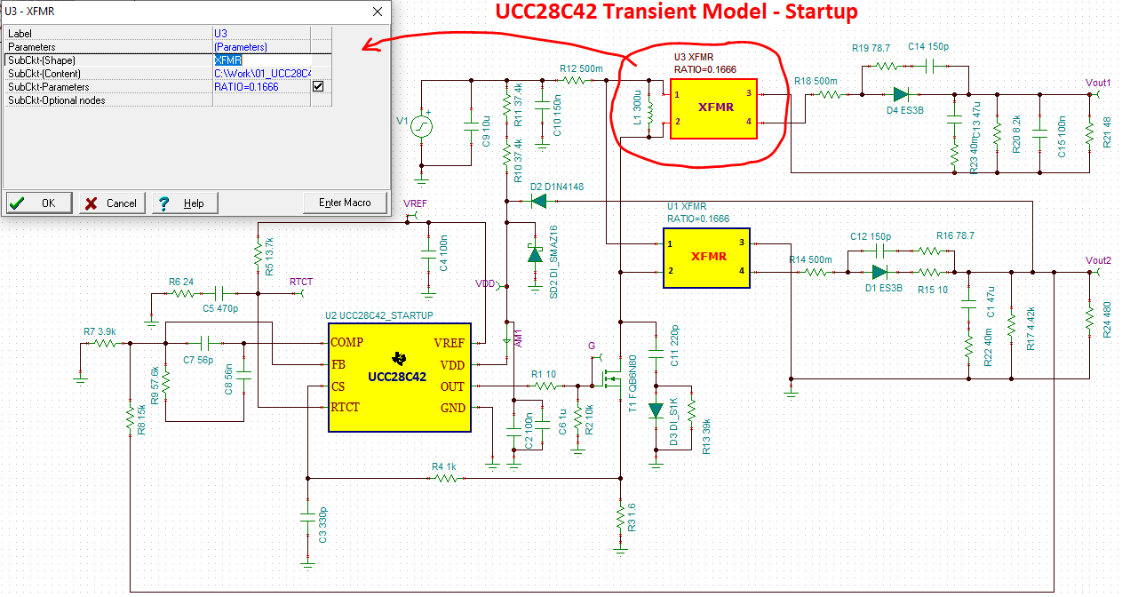
    Thanks for connecting through E2E. The TINA transformer model is represented as an "ideal transformer", compared to the Webench model which is trying to help you design a customer transformer. The transformer parameters listed from your Webench result will have to be lumped and represented in TINA. For example, the primary DC resistance is shown below as R12, secondary dc resistance is R18, transformer primary magnetizing inductance is modeled by L1 and if you wanted to simulate the effect of leakage inductance (not shown below) you could add a small series inductor at pin1 and/or pin 4. If you click on the transformer box, you see the only parameter we can enter is "RATIO" and this is where you need to use the turns ratio numbers from Webench. You could repeat this process for each additional winding.

    Regards,

    Steve M