This thread has been locked.

If you have a related question, please click the "Ask a related question" button in the top right corner. The newly created question will be automatically linked to this question.

CSD19531Q5A: CSD19531Q5A drain and source showing short in first time testing.

Part Number: CSD19531Q5A
Other Parts Discussed in Thread: CSD17581Q5A

Problem:

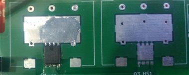
CSD19531Q5A Drain and source pins were showing short. When we unsolder and solder back, no issue. This happened 3 out of 5 times. The soldering was done by hand. 

1. Please let us know what could had caused the short with drain and source?

2. Does ESD or charge accumulation has anything to do with it? or is it purely soldering issue?

Thanks & Regards,

Macjan.

  • Hi Macjan,

    Thanks for your interest in TI FETs. I suspect you may have some soldering issues that may be causing the short between drain and source. Another possibility is that the gate may be floating high enough to turn on the FET if it is left floating when you probe drain and source. Please ensure the gate is shorted to the source when probing. You should always use proper ESD procedures whenever handling or working with these devices. The CSD19531Q5A passes 2000V HBM & CDM ESD testing. ESD damage to the gate can cause various issues including higher leakage, lower threshold voltage and catastrophic failure.

  • Sir,

    1. We are facing this problem when the power is OFF. The short looks like physical when we test it on multimeter.

    2. The solder short is not visible, it looks to be internal short.

    3. The short goes once it is re-soldered. ESD damage would had been permanent to the MOSFET. But in this case after re-soldering it works perfectly fine.

    Thanks & regards,

    Macjan

  • Hi Macjan,

    Thanks again for your interest in TI FETs. Even with the power OFF, you can still charge an open gate with a multimeter when probing the device. However, I agree that you probably have an external short underneath the package where it cannot be seen under a microscope. If you have x-ray inspection equipment you should be able to verify the short. Please make sure you're following the recommended PCB footprint in the datasheet. Below is a link to an app note on QFN and PCB attachment including rework instructions.

  • Sir,

    Sorry for the delay, we were waiting for higher current bench supply for testing.

    We carefully placed new Mosfet's on the PCB. The setup worked well on lower voltages below 24V. 

    Our application actually has voltage around 95V maximum. We turned ON inductive load ( 5 Lamps in series 5A current at 60V) and went up to 60V with no heat issues. So we turned OFF the load. 

    The new problem we found is that when we turned back ON the Inductive load again, the mosfet turned ON at 5A current load and started heating a lot. After turning OFF power completely we found mosfet is Drain and Source is short.

    The setup specs:

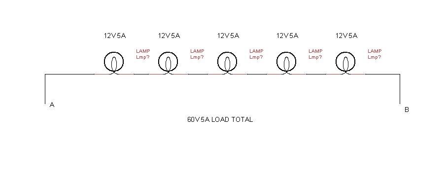
    Load lamps: 12V 60W OSRAM make connected in series of 5 to achieve 60V at 5A.

    Vgate = 15.8V for turning ON device.

    Bench supply: 65V, 5A max. rated.

    Testing conditions: 60V, 5A Load.  

    Please let us know what could  had cause this problem. 

    Thanks & Regards,

    Macjan

  • Macjan,

    Due to power cuts in Dallas due to severe weather John is not able to answer at the moment, he will be back online as soon as he can to answer.

  • Hello Macjan,

    Thanks again for your interest in TI FETs. From your description: VDS = VIN - VLOAD, ID = ILOAD and PD = VDS x ID. Up to 60V, there is not much voltage drop across the FET and not much power loss. However, as your input voltage is increased, there is additional VDS voltage drop across the FET and power loss goes up. At an input voltage of 65V, the power loss in the FET: PD = 5V x 5A = 25W which is in excess of what this package is capable of dissipating. Most likely, the FET is heating up and going into thermal runaway which is causing the FET to fail. Increasing the input voltage to 95V dramatically increases the power dissipation in the FET: PD = 35V x 5A = 175W. The 5x6mm SON package is capable of dissipating about 3W maximum on a multilayer PCB with a good layout.

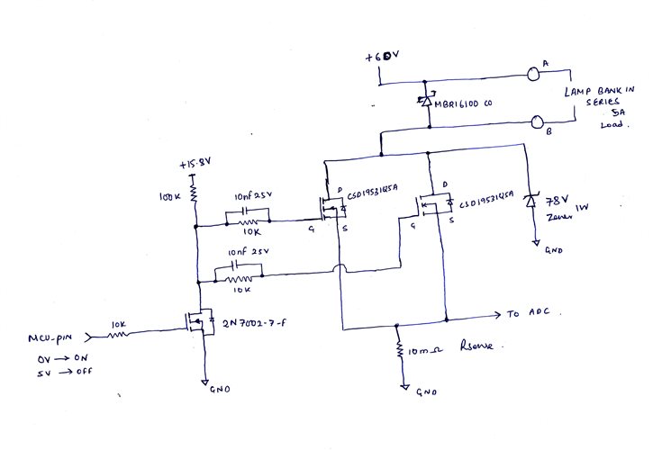
    Can you share your schematic? Perhaps my understanding of your application is incorrect. Below are links to some useful technical information on power dissipation of TI FETs.

    Other Parts Discussed in Post: CSD17581Q5A When starting a new design, engineers are often overwhelmed by the number of package options for power metal-oxide semiconductor field-effect transistors ( MOSFET…

  • Sir,

    Below is the schematic diagram of the connection.

    The load bank at point A, B looks like below

    When we tested the load bank at lower voltage of 50V, there was no heat across Mosfet, the load current was around 4.16A. We even tried turning ON/ OFF multiple times to see if back emf was a problem. But nothing happened at 50V.

    Power dissipation depending on Rds which is ~~ 5mOhm at gate voltage >10V.. Then  4.16 x 4.16 x 0.005 = 86mW which was true. 

    This mosfet is capable of running up to 100V according to datasheet. We raised the voltage to 60V gradually to check at 5A load current which works fine. However if we start same system with same load ratings at 60V, the mosfet behaved liked short and since then it was short even after power off and even after removing mosfet it showed short. 

    Calculation wise 5 x 5 x 0.005 = 125mW has to drop across mosfet and should had been stable. But for some reason Drain and source shorts.

    Some videos on youtube explain a phenomenon called avalanche breakdown of internal diode across PN of mosfet due to slow discharge of high back emf voltage across load when connected to inductive load. I hope its not what's happening here. 

    Thanks & Regards,

    Macjan.

  • Hi Macjan,

    Thanks for the update. I recommend capturing VGS and VDS waveforms with an oscilloscope at turn-on and turn-off of the system. Please capture multiple waveforms showing the rising and falling edges. You're not seeing any issues when the supply voltage is gradually increased with the FETs on but the failure occurs after system startup or shutdown. One or both of the FETs may avalanche during these transitions. TI specs single pulse avalanche in the datasheet. The other consideration may be an SOA (safe operating area) violation during turn-on or turn-off of the FETs. You have a large gate resistance, 100k + 10k at turn-on and 10k at turn-off. I'm including links below for more information on how TI tests and rates avalanche/UIS and SOA for our FETs.

  • Sir,

    I've conducted test as per your request. I've attached screenshots of DSO and multimeter readings of VDS and current as requested. 

    Till 50V, we tested multiple times switching ON/OFF using fix 10seconds delay for ON and 10seconds delay for OFF. Results are good. But when we changed to 55V, it just went in 1 try. I've attached photos. Please check and let me know on the observations.

    (Attached pdf : Page 6 - > Mosfet Failed)

    MOSFET_LOAD_TEST.pdf

    Thanks & Regards,

    Macjan

  • Hi Macjan,

    Thanks for sharing your test results. It does not appear that the FETs are being driven to avalanche. There is a spike at turn-off but VDS is not exceeding the breakdown voltage. Can you please zoom in on the turn-off transition to get a better picture of the voltage spike. What is the bandwidth of the scope? Is it possible to capture the current waveform by measuring the voltage across the 10mOhm current sense resistor? I'd like to see if there is overshoot/undershoot of the current. The turn-on transition takes longer due to the higher gate resistance (100k + 10k). It may be getting close to the SOA current limit of ~4A for 52V/1ms pulse width.

  • Hi Macjan,

    I have some additional comments. I cannot be certain when the FET failed. It may have occurred at turn-off at 52.5V or at turn-on at 55V. Did you check that the FET was OK after each time it was turned off?

    I'd like to close out this thread and move this conversation outside of e2e. I have sent you a friend request. As soon as you accept it, I will contact with a private message.

  • Sir,

    At 52.5V we tried turning ON/OFF mosfet multiple times. Had no issue. At 55V it failed directly at first turn ON. I also like to know what will be ideal gate resistance since you mentioned 100k+10k. I can try this for next test. Also let me know what exactly you want me to capture this time on DSO in details since I got only 1 shot to try this for every new mosfet.

  • Hi Macjan,

    I just sent you a private message with my email address. Please email me and we can continue this discussion via regular email.