This thread has been locked.

If you have a related question, please click the "Ask a related question" button in the top right corner. The newly created question will be automatically linked to this question.

Question on SS/ENA pin of TPS54310

Anonymous
Anonymous
Other Parts Discussed in Thread: TPS54310

Hi All,


I would like to ask a question on TPS54310 connection.


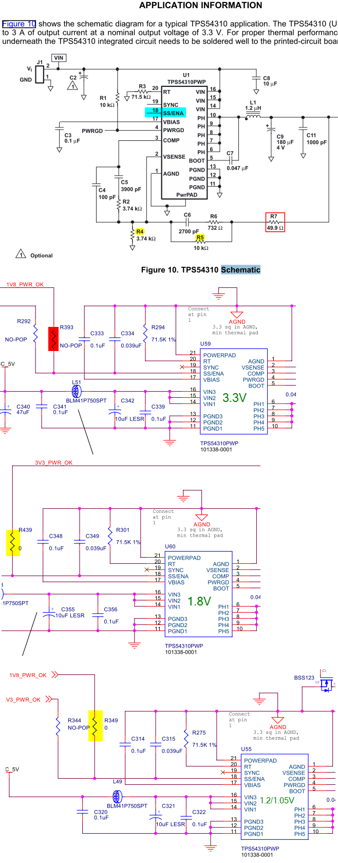
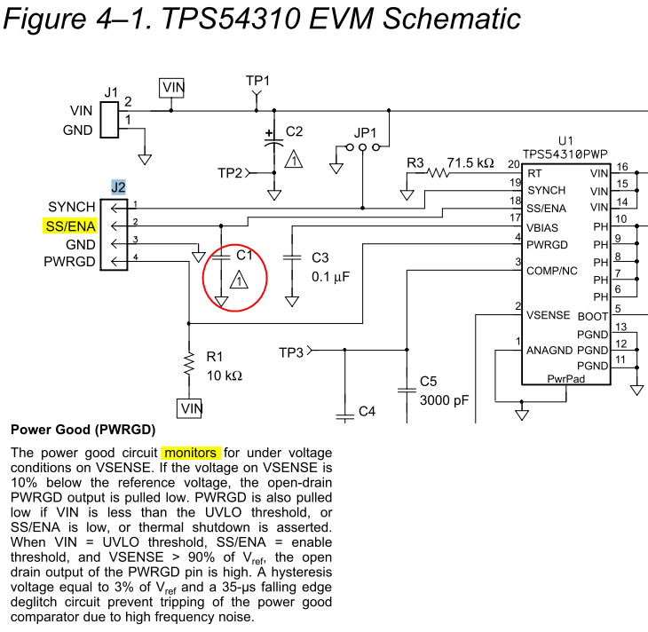
In the schematic shown in SLVS412d, the pin is unconnected. However, on EVM6437 which I am referencing, I found that the pin is connected on one TPS54310 and unconnected on another two:

1.     For TPS54310 output 3.3V, the pin is unconnected.

2.     For TPS54310 output 1.8V, the pin connected to 3.3V.

3.     For TPS54310 output 1.2/1.05V, the pin connected to 1.8V.


There seems to be some regularity here that regulators output lower voltage have their SS/ENA pins connected to regulators output higher voltage, in a cascading manner.


But why? Are they necessary? If I left all SS/ENA unconnected, will the system work?


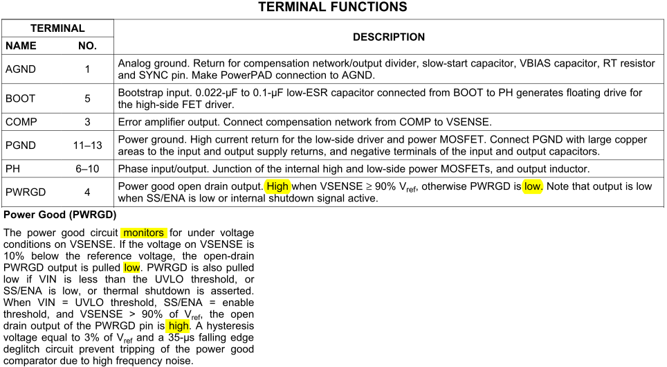
I went to page 12 (Slow-Start/Enable) for its detailed description, and there seem to be related to threshold issue. My guess on its purpose is that:

1.     By cascading higher voltage output to lower voltage output regulator’s SS/ENA pin, then power will be distributed to board devices in the same order, during the short time when the 5V supply is plugged in.

2.     This should be related to either

a.     Booting

b.     Reset

procedure.


Is this true?


Anyway, the most important question here is on their necessity. Do I have to connect SS/ENA in that cascading fashion to be able to use my board?


Thanks,

Zheng

  • There are 3 possibilities for SS/ENA:


    These first two use the "slow start" function of the IC:

    1. SS/ENA pin is open.  The converter will start up at the internal slow start rate. This is the case for the EVM.

    2. SS/ENA with capacitor to ground.  There is an internal constant current source that will charge the external slow start capacitor at a constant rate.  The output voltage will rise to the regulated output at that rate during start up.

    Enable function:

    3.  There is an enable function as well.  If you actively pull the SS/ENA pin low, the device is disabled.  Float or pull up above the EN threshold (1.2 V typ) to enable.  The most common use is to use the PWRGD function of an upstream regulator to enable.  yhat is likely what that design you reference was doing.

  • Anonymous
    0 Anonymous in reply to JohnTucker

    Dear John,


    I would still like to ask the following questions regarding your points:


    1.      The “EVM” here refers to TVP54310 EVM, not EVM6437, right?

    a.       I see in the TVP54310 EVM that SS/ENA is connected to J2, so the SS/ENA pin of J2 will be left unconnected?

    2.      In my attached picture in the first post, does SS/ENA in the 3.3V output regulator correspond to case 2?

    3.      From the description of PWRGD and its use in EVM6437, it is essentially a indicator designed to flag its internal status to other parts of the circuit?


    Zheng

  • Anonymous
    0 Anonymous in reply to JohnTucker

    Dear John,


    Another question is that how many stages of PWRGD cascade are allowed? If I am also have another 3.0V voltage to add within the current 3.3 – 1.8 – 1.2/1.05 configuration, may I simply “insert” it between 3.3 and 1.8? Does there exist a limit on the number of stages?


    JohnTucker said:
    1. SS/ENA pin is open.  The converter will start up at the internal slow start rate. This is the case for the EVM.
    3. There is an enable function as well.  If you actively pull the SS/ENA pin low, the device is disabled.  Float or pull up above the EN threshold (1.2 V typ) to enable


    Does the "open" in 1 and "float" in 3 mean the same thing, = unconnected?


    Thanks,

    Zheng

  • 1. Yes EVM refers to teh official EVM (SLVP201)  I do  not know what "EVM6437" refers to.  It is not an official EVM released by the product line.

    1a. J2 is a header used as test points.  You can connect SS/ENA to GND with a shunt to disable the IC.

    2.  It looks that way.  There ia a slow start capacitor from SS/ENA to GND and R393 is open. As I said I am not familiar with that schematic,  today is the first time I have seen it.

    3.  PWRGD goes high z when the output is within regulation.  You can use that as a control condition or as an input to voltage monitors etc.

  • If you are cascading PWRGD to SS/ENA (one PWRGD output feeds one SS/ENA input) there should be no limit.  Bear in mind that the previous voltage will need to complete its slow start sequence and be in regulation before the susbsequent voltage can begin its slow start sequence.  If using one PWRGD output to drive more than one SS/ENA, there may be some theretical limit as the open drain has to sink multiple SS charge current.  That current is small so ou should be able to drive any practical number (probably not 100 for instance).

    Open and Float are similar.  Open means "not connected"  Float means "not connected or actively pulled high or low".  In this case it is connected to a hi Z source (open drain output). 

  • Anonymous
    0 Anonymous in reply to JohnTucker

    Dear John,

    JohnTucker said:

    3.  PWRGD goes high z when the output is within regulation.

    I could find no information in the document saying that PWRGD can go hi-Z. All descriptions seem to suggest only two states. Could you explain in more detail?


    Zheng

  • The PWRGD pin is open drain.  To actually have it go high you will have to pull it up to an external rail

  • Anonymous
    0 Anonymous in reply to JohnTucker

    Dear John,


    I checked http://en.wikipedia.org/wiki/Open_collector, and noted that there seems to be a fundamental difference between NPN an MOSFET open drain collector:

    1.      For NPN, if internal output 1, then the transistor is on

    2.      For MOSFET, if internal output 1, then the transistor is off


    So in the case when

    1.      a pulling-up resistor is attached and when

    2.      PWRGD is high,

    Then if

    1.      NPN: external output low, SS/ENA regulator cut off

    2.      MOSFET: external output high, SS/ENA regulator on


    And because TVP54310 is made of MOSFET, so the cascading connection shown in the picture of the first post is correct. Is this the right explanation?


    Thanks,

    Zheng

  • For these parts, when PWRGD is not good, te internel FET is ON.  When the voltage goes into regulation, the PWRGD FET is turned OFF.  If it is connected directly to the TPS54310 SS/ENA pin, no additional pullup is required.

  • Anonymous
    0 Anonymous in reply to JohnTucker

    Dear John,

    I see it, thanks.

    Zheng