This thread has been locked.

If you have a related question, please click the "Ask a related question" button in the top right corner. The newly created question will be automatically linked to this question.

TPS43061: TPS43061 consumes large current on wakeup

Part Number: TPS43061

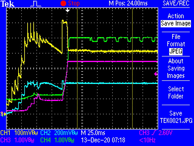
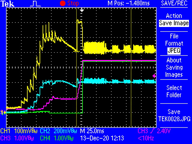
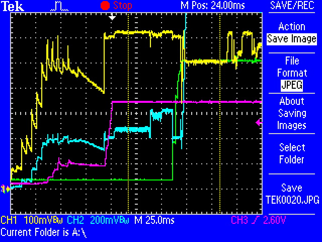
In the latest batch we've noticed that some TPS43061 devices on wake-up consume large currents from the VIN pin and do not functioning properly. The failure is intermittent (happens after multiple tries) and even when happens, the device eventually wakes up after a few seconds. When the failure does occur these are the symptoms that we see:
1. Large current consumption into VIN pin (>100mA)
2. EN pin remains low (internal pull-up not engaging)
3. VCC pin goes high immediately with VIN (normally the internal LDO should be disabled while EN is low)
4. SS remains low
5. HDRV pin goes high (to the same voltage as VIN)
Replacing the TPS43061 on one of the failing boards solved the problem. We would like to understand if this failure could have been caused by improper handling at the manufacturing facility, or whether there is another explanation to the failure.
Thank you

  • Hi Alexander,

    Could you show some key waveforms, and also your schematic?

    Thanks,

    Youhao Xi, Applications Engineering

  • Hi Xi,

    Unfortunately I cannot post a proprietary schematic in a public forum. I should be able to provide the schematic privately under NDA.

    I don't know if the waveforms are going to be very informative.

    This is an example of a failed wakeup. CH1 is the input voltage. CH2 is the output voltage. CH3 is irrelevant. CH4 is the voltage supplied to the VIN pin (separate from the converter input voltage) at a scale of 1V/div.

    Here I'm probing VCC pin voltage instead of VIN pin on CH4 during failed wakeup:

    The HDRV voltage also rises together with VCC. The EN pin is held low when I see the VCC and HDRV rise. During normal wakeup both VCC and HDRV are low when EN is low.

    From my analysis so far it looks like the TPS43061 received some kind of damage. I'm trying to figure out what kind of damage that could have been.

  • Hi Alexander,

    Understood about the schematic.  However, your pictures are corrupted which I cannot open.  Could you re-post?

    Thanks,

    Youhao

  • CH1: input voltage, CH2: output voltage, CH4: supply voltage (VIN pin)

    CH1: input voltage, CH2: output voltage, CH4: VCC pin

    A few details about the circuit:

    Input voltage: 0.5V

    Output voltage: 5V

    Load: no load

    Supply voltage (VIN pin): 5V

    Correct wakeup looks like this:

    CH1: input voltage, CH2: output voltage, CH4: supply voltage (VIN pin)

  • Hi Alexander,

    What are your scope probe attenuation ratio?  I read 100mV/div or 200mV/div from the scope picture, but what are the actual voltages for other signals like input voltage, output voltage?  I know you said VIN pin trace is 1V/div but the last picture does not seem turning on CH-4. 


    Thanks,
    Youhao

  • The probe ratio for CH3 and CH4 is 1V/div for all the captures

  • I may need to review your schematic.  Please send via the PMS which I have made a friendship request in PMS.  Please accept and share the schematic.

    Also, please note that the current pin need to see >3V for guaranteed operation.  Make sure it is satisfied. 

    Thanks,

    Youhao

  • Hi Alexander,

    Since we are communicating through PMS, and not update from you for two weeks, may I assume the issue is solved so I can close this thread?  You are welcome to re-open it by adding a new post.

    Thanks,

    Youhao