This thread has been locked.

If you have a related question, please click the "Ask a related question" button in the top right corner. The newly created question will be automatically linked to this question.

TPS54302: SW node absolute max & dead time

Part Number: TPS54302

Hi 

Could you please let me know the dead time between high side FET off and low side FET on, and Low side FET off and high side FET on?

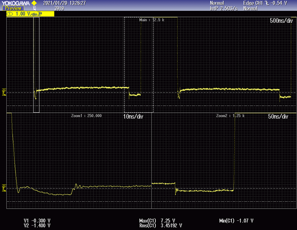
Negative voltage(around -0.6V) on SW node during dead time was measured over 50ns(absolute max, transient time) .

I think, those negative voltage are internal operation during dead time. so it is no problem because it is not external apply voltage. is it correct?

Also, is the dead time on the waveform normal?


Thanks

Muk

  • Hi,

    Normally the deadtime is around 10ns . You can refer below waveform .

    for the Absolute Maximum Ratings of the SW Node, this minimum voltage rating found in the data sheet is actually a dc rating and means that the part could be damaged if a constant voltage below –0.3 V is applied at the SW node from a source other than the output inductor during switching operation.

    you also find the detailed explanation from the application note: http://www.ti.com/lit/an/slva494a/slva494a.pdf

    BRs,

    Young