This thread has been locked.

If you have a related question, please click the "Ask a related question" button in the top right corner. The newly created question will be automatically linked to this question.

Question on TVP54310 thermal pad

Anonymous
Anonymous

Hi All,


I would like to ask a question on TVP54310.


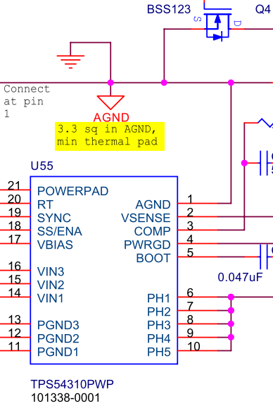
What does the highlighted texts in EVM6437 schematics mean? Is “sq” an area unit (square xx, etc.)? What does the “thermal pad” refer to? Do I have to buy any additional thermal pad, or TVP54310 already embeds it?


Thanks,

Zheng

  • Tat is requiring a minimum of 3.3 square inches of copper area connected to the exposed powerpad under the device.  For pest results, that copper should be on teh back side and conneted to the powerpad area on the top side with thermal vias.  BTW, you keep referencing EVM6437.  What is that design? Where did you get it?

  • Anonymous
    0 Anonymous in reply to JohnTucker

    Dear John,

    EVM6437 said:

    3.3 sq in AGND, min thermal pad

    so according to above, the copper area needs to get connected to AGND net?

    And according to you that the copper area should be placed on the back, so this is conceptually and functionally different from internal plane's large copper area which are used to provide stable reference voltage?

    EVM6437 is a EVM for DaVinci 6437 by Spectrum Digital.


    Zheng

  • That is according to that reference design, I suppose it was tested and checked, but I have no firsthand knowledge of it.  When I design using these parts, I tie the power pad to the internal ground plane if one exists.  I tie the AGND pin to the thermal pad area as well with a single trace directly under the IC.  I tie the sensitive analog returns (v feedback, RT, SS/ENA, etc to the AGND pin with a dedicated trace on teh top side.  For 3 amp designs that is probably sufficient, but our EVMs almost always have some copper on teh back side directly under the device connected to the exposed pad area by thermal vias.  Copper on teh outer (front and vack side) are more efficient at transferring heat to the ambient air.


    If you want to follow that reference design, you should contact the designer directly.

  • Anonymous
    0 Anonymous in reply to JohnTucker

    Dear John,

    I will consult experienced designer on this, thanks very much.

    Zheng

  • Anonymous
    0 Anonymous in reply to JohnTucker

    Dear John,

    I posted a new question at http://e2e.ti.com/support/dsp/davinci_digital_media_processors/f/99/t/98000.aspx in which I suspect EVM6437 PCB design uses thermal relief via connection to connect PowerPAD of TVP54310 to internal plane, and it should be a design fault. Could you have a look at the post?


    Zheng

  • You definitely get better heat transfer with a solid connection.  Thermal releif connections are just that, to inhibit heat transer, not to facilitate it.  That reference design may still have sufficient thermal path, I did not work on or do any testing with that design.  For your purposes, I highly recommend that you use the solid connection.

  • Anonymous
    0 Anonymous in reply to JohnTucker

    Dear John,

    I got it, thanks very much for this confirmation.

    Zheng