This thread has been locked.

If you have a related question, please click the "Ask a related question" button in the top right corner. The newly created question will be automatically linked to this question.

BQ76940: Several non-adjacent cells open balancing

Part Number: BQ76940

Hi Team,

Our team is using BQ76940 to develop products, and we have some problems in battery balancing and need help from you.

In the 1-5 group, the 1 3 5 cell balance is turned on at the same time, and the 5 cell balance cannot be turned on. The same is true in the 6-10 group.But it is feasible to turn on each one separately

This is related to our balanced circuit diagram.


We measured the gate of the N-MOS with an oscilloscope yesterday, and we got the following waveform when the 5 cell were individually balanced


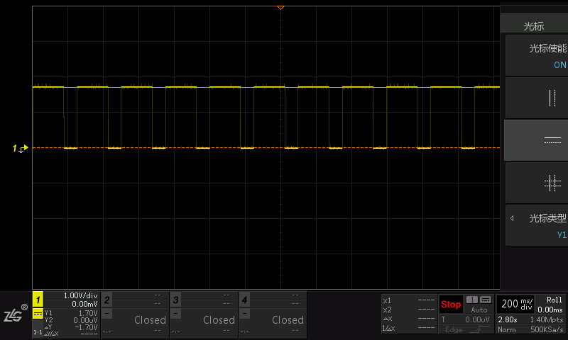
The time occupied by his high level and low level is in accordance with the specification, the total period of 250ms, 175ms balanced time 70%.

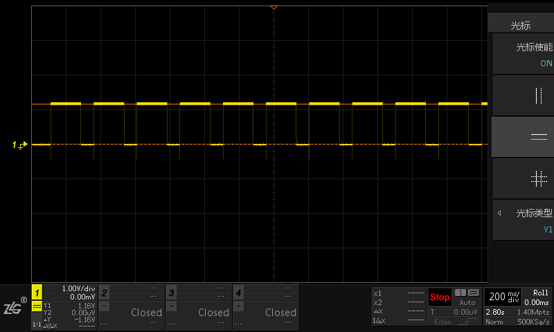
You can turn on the balance of the 3 and 5 batteries at the same time. This is their waveform, and the time period is correct, but the voltage drops to 1.2v.


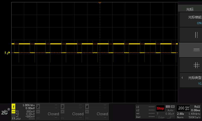
But when we turn on the balance of 1 3 5 batteries at the same time, 1 3 can work normally, and 5 cannot. The following is the waveform diagram of No. 5 at this time, the time period is correct, but the voltage has dropped to 0.7v, this voltage can no longer make the N-MOS tube turn on.


In the data sheet, we only see that two adjacent batteries should not be balanced together, and there is no explanation for how many are turned on at the same time. Whether only two batteries are allowed to be balanced in each group of 1-5, 6-10, 11-15 , Or because of the problem of our equalization circuit, the output capacity of the chip is reduced.

Expect for your kindly reply, thanks.


Best Regards


  • Hi Tianxia,

    The schematic clip is small.  I see you have Zener diodes across each pair of inputs, and for the low inputs of each group.  I can't read the values.

    When a cell balances, the adjacent cell inputs see an increased voltage.  For example with 4V/cell, balancing cell 1 will pull VC0 and VC1 to about 2V, and the 2V is available to the external FET for Vgs. the difference between VC2 is at 8V and VC2 - VC1 is about 6V.  The Zener diode should not conduct.  When cell 3 is also balanced, VC3 and VC2 will pull together to about 10V.  The difference between VC2 and VC1 is now 10 - 2 = 8V.  If the Zener is conducting the voltage will not be as high on VC3 & VC2, and higher on VC1 & VC0.  The bottom cell's FET gets a little more Vgs, the upper cell gets a little less.

    When cell 5 is balanced also VC5 and VC4 pull together also, they would want to go to 18V.  Again if the Zeners don't restrict movement the voltage between VC4 and VC3 will be 18 - 10 = 8V.  If the Zener diodes conduct and reduce that voltage VC0 & VC1 are pulled up more again increasing the Vgs for that FET, the cell 3 FET sees a medium Vgs, the cell 5 FET sees a reduced Vgs.  From the description this may be the phenomena you are describing. 

    Check the voltage rating of the Zeners, if they are conducting you might increase the level.  There is little margin between the voltage on the cells with every other cell balancing and the abs max differential voltage of the inputs to position a Zener with tolerance.  You may need to compromise on the number of FETs which can balance simultaneously.

  • Hi,

    Thank you very much for your reply and help, it has played a great role to us, we will make changes according to your suggestions, and the results should be available tomorrow.

    Best Regards