

Hi Sir,
My customer is creating DFMEA for the following devices.
Could you please clarify this technical inquiry?
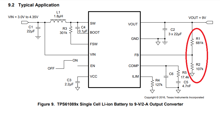
・TPS61089RNRR
R1=330k、R2=36k
・TPS62160DSGR
R1=220k、R2=68k
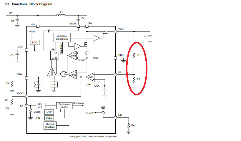
Resistors R1 and R2 connected to FB terminals according to the recommended schematic in the datasheet.
1) R1 open
If the FB terminal is connected to GND at R2 (≒Vref), what voltage will the Vout becomes to?
(is this value depends on the gain of the Gm (depending on the feedback resistance)?)
If you have a formula to calculate from R2, please let me know.
2) R2 open
If the FB terminal is connected to GND at R1 (≒Vref), what voltage will the Vout becomes to?
(is this value depends on the gain of the Gm (depending on the feedback resistance)?)
If you have a formula to calculate from R1, please let me know.
Thanks a lot.
