This thread has been locked.

If you have a related question, please click the "Ask a related question" button in the top right corner. The newly created question will be automatically linked to this question.

LM5122-Q1: Open Loop Response

Part Number: LM5122-Q1
Other Parts Discussed in Thread: LM5122

Hi team,

Good day.

Based on the LM5122-Q1 datasheet, the open-loop response transfer function is defined as,

Our customer have three questions regarding this transfer function:

1. Is this open-loop response part of a unity feedback system?

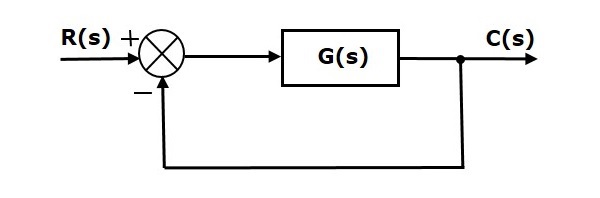
If so, is the given open-loop response includes the plant? (in this case, the plant is the boost converter circuit controlled by the LM5122).


2. What two quantities does this transfer function relate to? For example, the transfer function for a boost converter circuit alone typically relates V_out and V_in as a function of duty cycle.


3. The customer is simulating this system (a boost converter circuit controlled by the LM5122) using MATLAB. Will using MATLAB's >>margin() function on the given open loop response transfer function yield valid results for the phase and gain margins of the system?

Thank you in advance!


Regards,
Carlo

  • Hi Carlo,

    1. It's not a unity gain system. It has the feedback gain H(s) as well. The "open loop response" T(s) here refers to G(s)H(s), as it appears in the denominator of the output/input transfer function. G(s) is the plant so it includes the plant for sure.

    2. This function does not associated input/output. You can also interpret it as the loop response which means if you inject signal at one point, what you will get as the output at the same point through the whole loop. T(s) is used to simplify the feedback analysis in frequency domain. Details are discussed in classical control theory.

    3. That is correct.

    Please let me know if they have any question.

    Thanks,

    Yinsong

  • Hello Yinsong,


    Thank you for looking into this.

    Regarding question 1, would this means that the closed-loop transfer function will be equal to [ T(s) ] / [ 1 + T(s) ]?

    For question 2, since there is no associated input/output, is simulating the response to an input (for example, a step input) will not yield a meaningful result? Is there a way to simulate step loading using the given transfer function?


    Regards,
    Carlo

  • Hi Carlo,

    1. No, it would be G(s)/(1+T(s)). FYI, the rule of closed loop transfer function is to put the plant in the numerator and loop gain in the denominator.

    2. There will be no physically meaningful result if they use T(s) as the output/input transfer function to get the time domain response. To get the correct step response, they need to use the transfer function presented in 1.

    Thanks,

    Yinsong

  • Hello Yinsong,

    Good day.

    1. When you refer to G(s) as the plant, I want to confirm that you are referring to the transfer function of the circuit itself. (That would be V_out / V_in = 1 / (1-D) where D is the duty cycle for an ideal boost.) If not, then what is the equation of that plant that you are referring to?


    2. If a step response in the time domain can be simulated using G(s) / [ 1+ T(s) ], what does it mean? For example, is it the response to a step-change in load resistance?


    Regards,
    Carlo

  • Hi Carlo,

    1. G(s) does refer to Vout/Vin. However, it is not 1/(1-D). 1/(1-D) is the large signal DC ratio. For the loop estimation of switched-mode power supply, we always look at the AC small signal. For a Boost converter, it contains a low frequency pole, an ESR zero, and a RHP zero. For current mode control applied in LM5122, it also contains the half switching frequency double pole due the sampling effect.

    2. It means if there is a step on the input voltage, what response will appear on the output voltage. However, as mentioned in 1, it is the small signal model and not necessarily apply to the large signal.

    Thanks,

    Yinsong

  • Hi Yinsong,

    Thank you for your reply. Our customer has the following additional questions:

    1. Do the modulator and feedback transfer functions are given in the datasheet correspond to G(s) and H(s) in the attached screenshot? If so, what do the inputs and outputs R(s) and C(s) represent? If not, would you be able to provide a block diagram to make it more clear?

    2. We followed the recommendations for loop compensation components in 8.2.2.19 and we got a system with about 1 degree of phase margin and 1 dB of gain margin. Is that a reasonable result? If so, what approach would you recommend for increasing the gain and phase margins of the system?

    3. In Table 2 on page 29 of the datasheet, the comprehensive formula for the high-frequency pole in the feedback transfer function looks like it has a typo. Can you please confirm what the formula should look like for the high-frequency pole?


    Your continued assistance is appreciated.

    Regards,
    Carlo

  • Hi Carlo,

    1. Sorry for the confusion. That is essentially correct. The input R(s) represents the perturbation source which we would like to investigate. It is usually input voltage or output current. The output C(s) is the output voltage.

    2. That is not good. We usually need >45 deg phase margin and >10dB gain margin at least. Do you know what are their Rcomp, Ccomp, and Chf values?

    3. Are you talking about this one? 1/(Rcomp*(Ccomp||Chf)) Why do you think there is a typo?

    Thanks,

    Yinsong

  • Hi Yinsong,

    There have been no follow-up questions from our customer. The post can now be resolved.

    Your assistance is appreciated.


    Regards,
    Carlo