Hi,
We have designed a cascaded power suply module including TPS40200 and have a little problem with it.
When we assemble the circuit with Switcher Pro calculated components it did not work as expected. When I incerese the Css, say 1uF, it works but another problem arises.
Could you please help me to solve my problem?
Here is the details;
1 - Desired function ; 34V to 49V input ==> 27V@1.5A output
2 - First off all I have only assembled the TPS40200 circuit components to isolate problem. (No cascading)
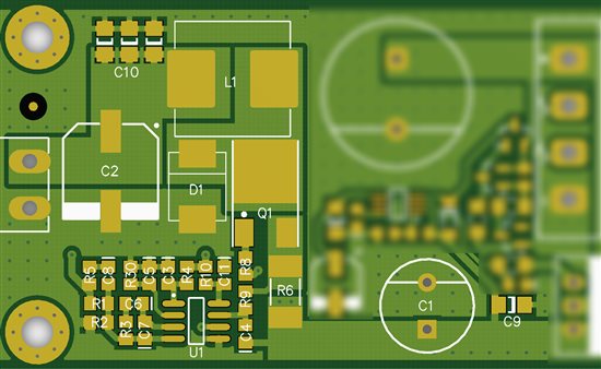
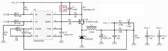
3 - I have designed PCB before Switcher Pro update, so R10 is placeed where the previoud version advice. Location of the R10 can be real problem ?
4 - Started with Switcher Pro calculated components and there was no expected output; 1.5V with 220 Ohm load, unstable approx 21V with no load.
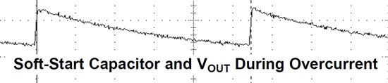
Wave form on the SS pin was the same with overcurrent situation as described in datasheet. (1.7Vpeak when unloadaed, 1Vpeak with 220 Ohm load)
When I increase the Css value to approx 1uF it works fine with resistive load as expected. It is also works with cascaded LDO (24V, no soft start)
But it does not work with intended load neither single nor cascaded. Intended load can be any type device with switching regulator. 27V output can be
generated but not stable.
5 - I have added a added a resistor parallel with the Css to decrease discharge time. Played with the resistor value but it does not solve problem.
6 - Played with R8 resistor value, compansation components (accorging to Switcher Pro), no way.
7 - I have removed R9 and shorted C4 to disable OCP but it did not worked even if unloaded.
8- I have suspected with PCB and components and try with 6 different setup, but all the same.
9- Can PCB layout be a problem ?
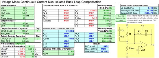
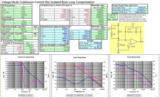
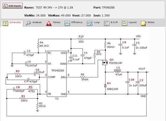
Switcher Pro schematic;
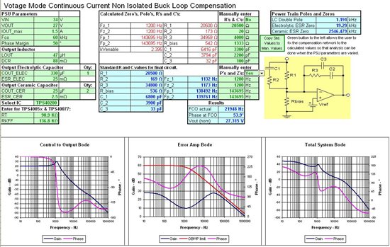
Applied schematic;
PCB layout; (Two layer, bottom for power gorund)