Dear TI community,
I just read the following topic: https://e2e.ti.com/support/tools/sim-hw-system-design/f/234/p/616938/2272973?tisearch=e2e-sitesearch&keymatch=TPS50601-SP%252525252525252520spice#2272973
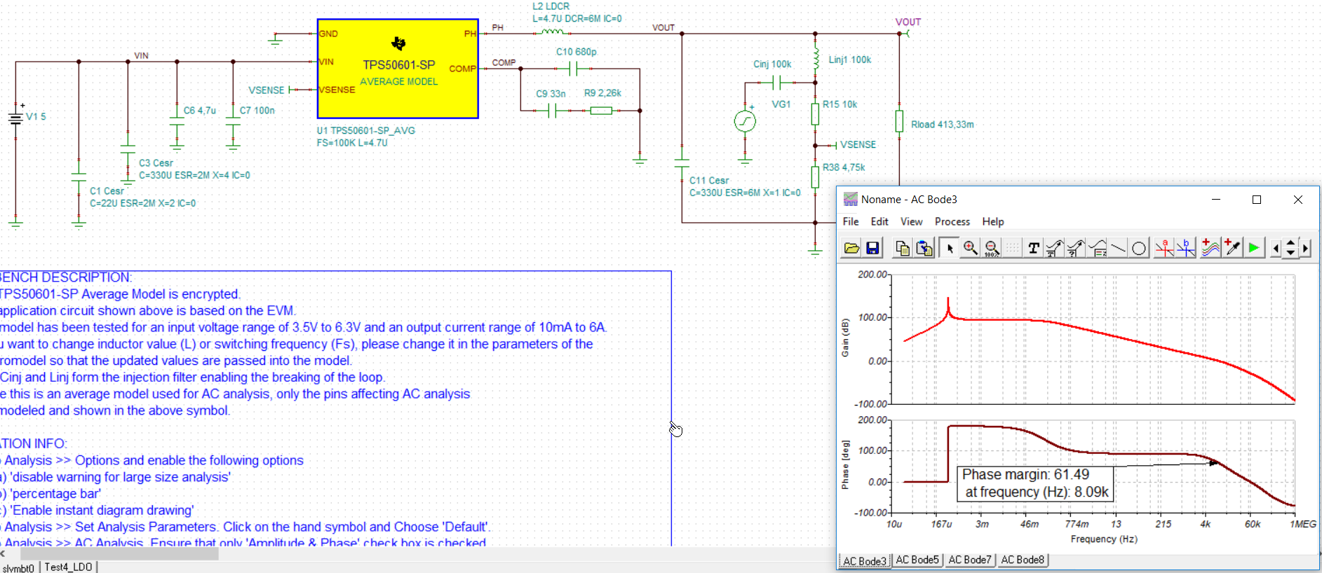
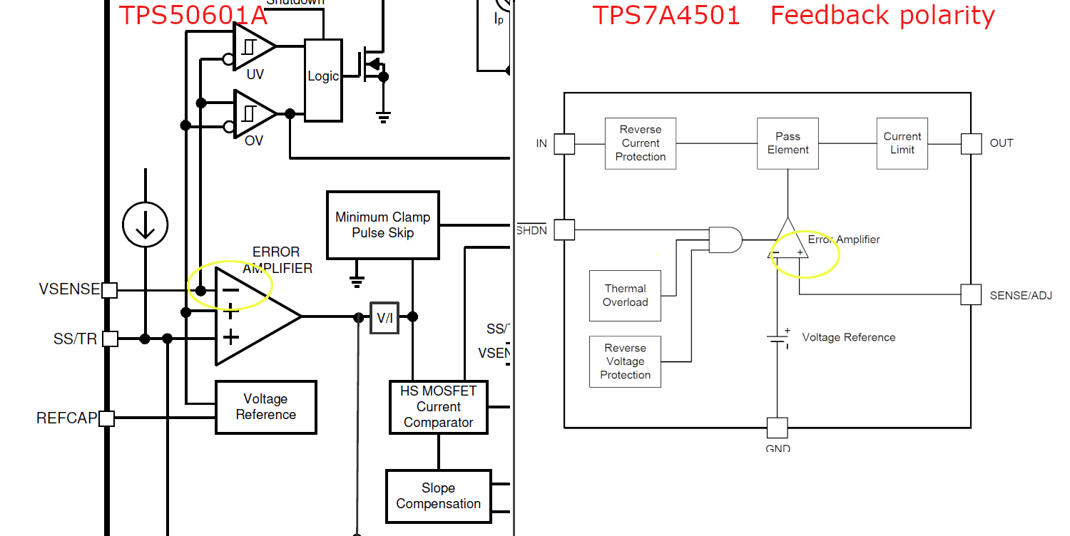
Which helped me understand why there is a +180° shift at the beginning of the graph. According to the post, this is because the loop gain transfer function does not include "-1" factor due to the negative feedback at the error amplifier. Consequently, the phase margin is computed with respect to 0° instead of typical -180°. I've tried to reproduce this example and I had the same result. This can be seen in my first screenshot below.
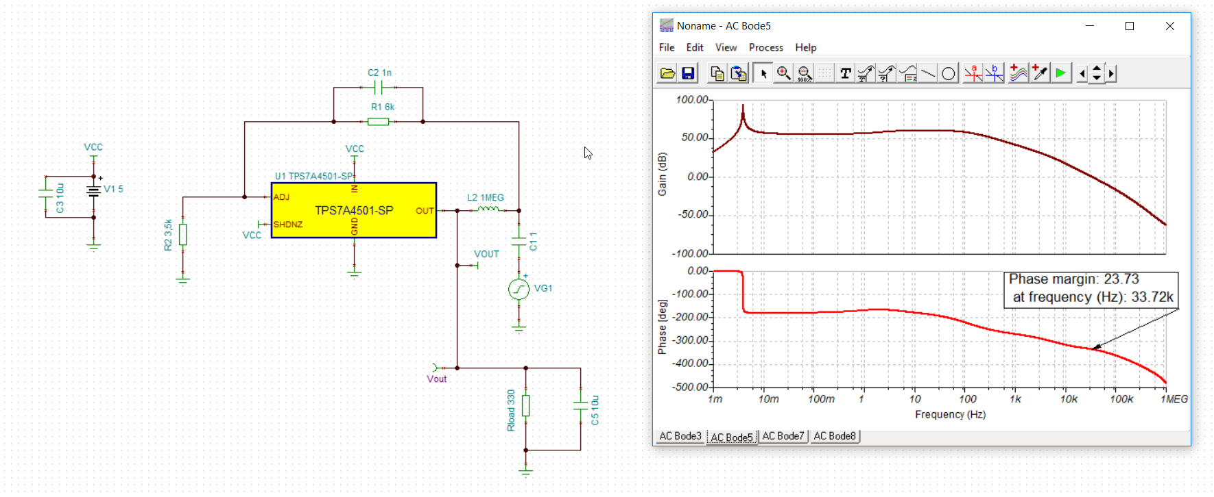
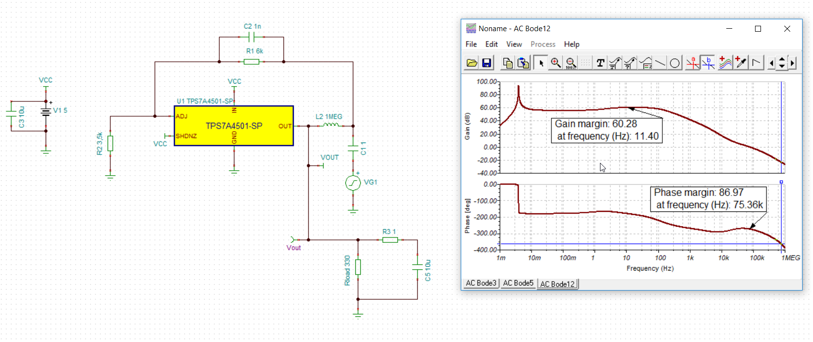
Nevertheless, the device I am interesting in simulating is the LDO : TPS7A4501-SP. I used the Worst-Case Analysis model. The simulation result can be seen in my second screenshot below.
So in this case, why is there a phase shift of -180°? I don't really understand, theoritically, where does this shift come from? Shouldn't it be the same as the shift for the TPS50601 simulation?
Thank you in advance for your answer.
Kind regards,