This thread has been locked.

If you have a related question, please click the "Ask a related question" button in the top right corner. The newly created question will be automatically linked to this question.

TPS549B22: default Vout setting

Part Number: TPS549B22
Other Parts Discussed in Thread: TPS546D24A

HI TI expert,

we would like to use TPS549B22 for our design to meet the following requirement:

default Vout=0.84V and need adjust the output voltage on the flying.

I plan to do the design as following:

1. set Vsel=0.75V by RVSEL=16.5Kohm according to the datasheet page20 table 2

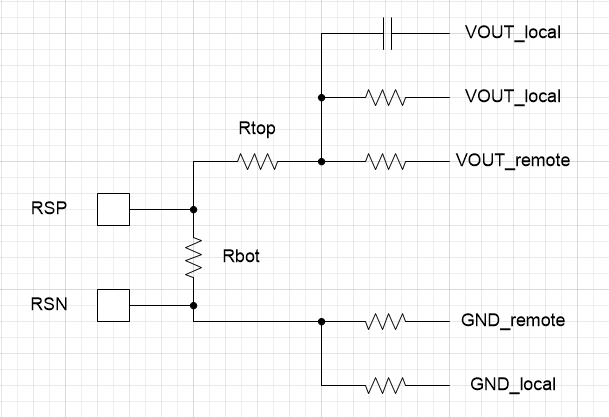
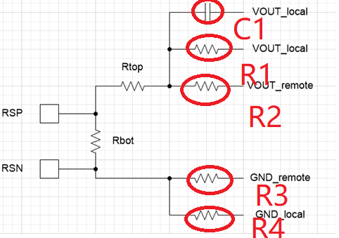
2. resistor=82.5K between RSP and PSN, RSP connects to Vout by a resistor=10K

I read some E2E tickets, and found a comment: The TPS549B22 always boots to the voltage defined by the VSEL pin.

Questions:

a) Does it means for my designthe Vout  will go to Vsel=0.75V firstly during bootup?

b) after power on, CPU is possible to adjust the Vout by VOUT _COMMAND. Can the default Vout be changed by VOUT_COMMAND and storing that value to NVM using STORE_DEFAULT_ALL? 

  •  

    a) Does it means for my designthe Vout  will go to Vsel=0.75V firstly during bootup?

    [PJM] No.  It means that the VOUT_COMMAND and the RSP to RSN voltage will always boot-up to 0.75V regardless of the last VOUT_COMMAND value stored to NVM.

    b) after power on, CPU is possible to adjust the Vout by VOUT _COMMAND.

    [PJM] Yes, the RSP to RSN voltage can be changed via VOUT_COMMAND after power-up, but with an external resistor divider from VOUT to RSP, the output voltage will not follow the standard VOUT = VOUT_COMMAND x 2^-9V scaling.  The output voltage will follow a scaling of:

    VOUT_COMMAND x 2^-9V x (1-Rtop/Rbot)

    Where Rtop is the resistor from VOUT to RSP and Rbot is the resistor from RSP to RSN.

    This is also equal to Vout/Vsel x VOUT_COMMAND x 2^-9V

    Where Vout is the default output voltage (0.84V) and Vsel is the selected default reference voltage (0.75V) .

    For 0.84V output with a 0.75V default reference, that gives VOUT_COMMAND and LSB value of 2.188mV instead of  the standard 1.953mV

     Can the default Vout be changed by VOUT_COMMAND and storing that value to NVM using STORE_DEFAULT_ALL? 

    [PJM] the power-up default output voltage and initial VOUT_COMMAND value can not be changed by changing VOUT_COMMAND and using STORE_DEFAULT_ALL when VSEL is connected to a 100k / 16.5k divider.

    For an integrated FET converter that can:

    1) Program the initial output voltage to 0.84V

    2) Adjust the default output voltage by storing an updated VOUT_COMMAND value to NVM

    3) Continue to use the standard -9 Exponent ULINEAR16 format for VOUT_COMMAND

    You could consider the TPS546D24A, which offers a PIN_DETECT_OVERRIDE command that allows the user to direct the TPS546D24A to use stored NVM values on future power on resets, overriding the Pin Detection.

  • Thanks Peter.

    1. About your saying: For 0.84V output with a 0.75V default reference, that gives VOUT_COMMAND and LSB value of 2.188mV instead of  the standard 1.953mV. I didn't find the description in the datasheet., LSB value is 1.9531 mV and is read only, and can't be overwrite. Why did you say LSB value is 2.188mV instead of  the standard 1.953mV?
    2. Due to the diviver between RSP and RSN, how to route the trace of RSP and PSN as differentional?  Should VOSNS and RSN be routed as differential according to picture showed below?

  •  

    Unfortunately your images did not come through correctly, so I can't comment on the images.

    However:

    1) Yes, VOUT_MODE is read only and can not be changed, and the LSB from VOUT_COMMAND to RSP - RSN is still fixed at 1.9531mV / LSB, but since VOUT is not directly connected to RSP, the LSB of VOUT is not 1.9531mV, but is 2.188mV since ever 1.9531mV on RSP - RSN translates to 2.188mV at VOUT.

    2) Below should be an image of how to route VOUT sense points back to RSP and RSN.  In this example there are 3 VOUT sense points.  There is a local resistive VOUT sense point for VOUT and GND, close to the output of the TPS549B22 converter and a remote resistive sense point.  The TPS549B22 will regulate the output voltage based on the average between these two, weighted by their sense resistance.  Typically designers will select a resistor value 10x higher for the local sense so that the remote-sense can maintain an accurate regulation voltage at the final output voltage.

    There is also a capacitive connection to the local output.  This is useful when there is resistance and inductance in the power delivery path between the TPS549B22's local output and the remote sensed output close to the load.  The capacitor allows the converter to compensate for the power-path delay and stabilize the full loop despite the phase lag introduced by this parasitic power-path filter.

  • THanks Peter.

    What is the recommended value of your attached sense circuit? 

  • HI Peter,

    can you please help to  review my schematic design? Thanks 

  •  

    Typically R2 and R3 (Remote Sense Resistance) is fairly low, between 10 and 50 ohms.  10-Ohms is typically a good value to select.

    R1 and R4 is generally 10x R2 and R3, 100-ohms to 500-ohms.

    C1's value really depends on the layout and the parasitic inductance and remote capacitance.  C1 might not be populated at all, or it may be sized to form a zero with R2 to shift to local feedback at high frequencies.  Typically the zero is located just below the poll created by that parasitic filter.

  •  

    The schematic looks pretty good.  I see an estimated 10mV of output ripple and 27mV of transient deflection on the output voltage on a 20A load step, so make sure those meet your requirements.