This thread has been locked.

If you have a related question, please click the "Ask a related question" button in the top right corner. The newly created question will be automatically linked to this question.

TPS7A52-Q1: SPICE model bugs

Part Number: TPS7A52-Q1
Other Parts Discussed in Thread: TPS7A52

I found a couple of bugs with the unencrypted SPICE model this device.

1. The text file, line 34, is missing a comment character.  This prevents TINA from importing the model- please fix this.

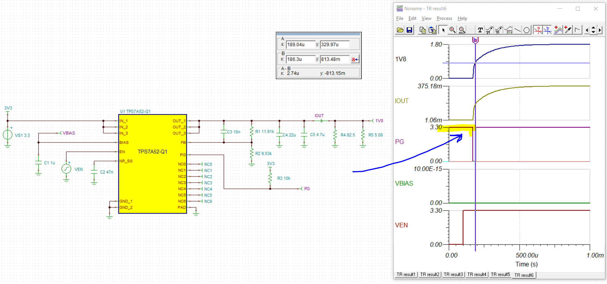
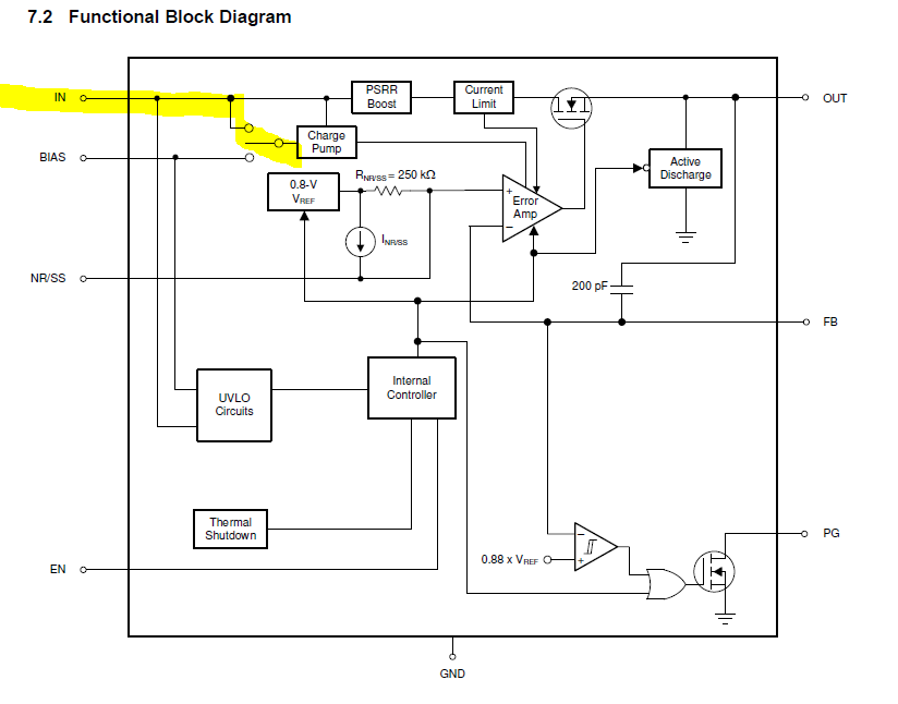
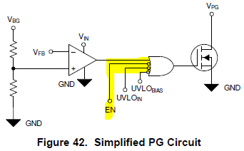
2. The PG logic is not simulating correctly.  When EN is low, PG should be low per Fig 42:

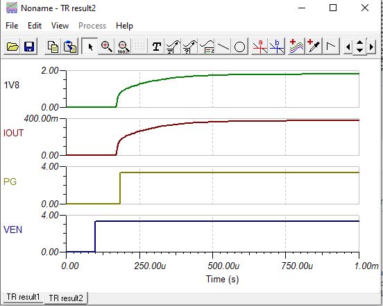
I have imported into TINA per following example.  I have attached the TINA simulation that includes the model should someone need it.

 TPS7A52-Q1.TSC

  • Hello,

    Thank you for the feedback.  We are aware of the missing comment in many of these legacy Spice models, and we make corrections to them as we locate additional models which have this issue.  We'll add this to our Spice model correction log.

    Regarding the TPS7A52 PG pin, the Spice model is simulating this correctly.  When there is no power applied to the device, as in the provided simulation, the internal circuitry cannot turn on the open drain MOSFET of the comparator circuit.  The PG pin looks like a very high impedance to ground in this case.  A voltage divider forms from the 10 kilo-ohm resistor and Rds_off of the MOSFET, which leaves approximately 3.3V on the PG pin.  For completeness I tested this on an EVM and confirmed that is what you will see.

    Thanks,

    - Stephen

  • Stephen-

    I disagree regarding the PG pin.  What I have attached I created myself from scratch, so not sure if you simulated some other deck.

    In simulation, 3.3V is provided all the time via VS1.

    The simulation calculates the initial operating point with VEN held low at time t=0.

    The VBIAS supply is reading zero because the internal switch is selecting VIN=3.3V, see figure in section 7.2 of Data sheet:

    That said, it does appear that I did not terminate the BIAS pin properly.  According to the data sheet if not used, the BIAS pin should be left floating or grounded.  When I ground the pin I get the same response on PG:

    I have attached the corrected version of the simulation.  Please run it and let me know what I need to do to get PG to simulate correctly if indeed the model is correct.

    -Steven2146.TPS7A52-Q1.TSC

  • I believe you that the actual device behaves properly, the issue is the simulation model.  Please see my follow on post.

    -Steve

  • Hi Steve,

    I mistakenly thought Vin was tied to Ven; I see now that is not the case.  The PG pin should be initially low as you have stated.  I'll check in the netlist to see if there is an easy mod to correct this; if not, we can add a simple mod outside of the IC to compensate for it.  Please give me some time to review this and get back to you.

    Thanks,

    - Stephen

  • Hi Steve,

    Okay give this a try, I've included the modified TINA simulation file at the bottom.  The mods include 2 altered lines of netlist code and one additional line of code.  The result is a simulation which more accurately reflects the PG functionality in your simulation.  If you don't see any additional issues, then we'll work to release this updated version onto the web.

    Here it is in Cadence:

    And here it is in TINA for your example circuit:

    Thanks,

    - Stephen

    /cfs-file/__key/communityserver-discussions-components-files/196/2146.TPS7A52_2D00_Q1_2D00_1.TSC

  • Thanks, that looks a lot better- I imagine it was a one-line change in the deck. Hopefully you can get the model on the web updated.

    -Steve