This thread has been locked.

If you have a related question, please click the "Ask a related question" button in the top right corner. The newly created question will be automatically linked to this question.

UCC21750: Random glitch in OUTH which switch the SiC Mosfet

Part Number: UCC21750

Hi,

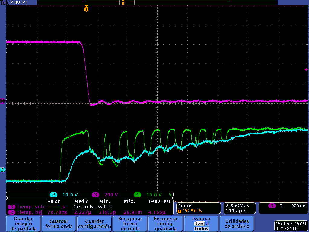
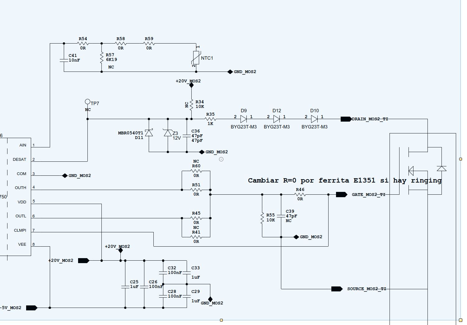
I am currently workin in a 250kW SiC inverter using the UCC21750 to driver the SiC Modules. In some occasions (ramdomly) we see a gitch in the ouput of OUTH and OUTL which turn on and off the MOSFET. At the beginning we thougth it was caused by the parasitic current flowing through Cgd due to the dvdt, but now we have changed our mind and we think it is caused by the driver since it is the OUTH and OUTL which are pulling down or pulling or up the gate signal with high frecuency oscillations.

We also see the same effect in the followin simulation.  To avoid this high frecuency oscillations we could increase the Cgs with an external capacitor (330nF) but this would increase the power required to drive the driver and we are not allowed.

Any idea where this effect is coming from?

Thanks in advance

  • Hi, Joan, Have you already built a prototype and tested it? Do you have any scope shots from the board if so?
  • Hello Don,

    Indeed we have a prototype and we the same effect in real life. The attached figure shows in channel 2 the signal measured in the gate of the SiC module, in chanel 4 the Vds of the module, and in channel 4 the OUTH of the UCC21750.  In fact, we saw this effect first in real life and trying to find out what was the reason, we made the simulation and realized that the same effect can be seen in the simulation.

    This figure shows the signals of the Low side mosfet of on of the three phases of the inverter. The Ron and Roff are 2.2Ohm

    The schematic is the following

  • Hi Joan,

    Thank you for the detailed information. From the waveform it seems like the gate driver is being properly turned on, but supply collapses when turning on the gate of the SiC FET. Gate oscillations could be due VDD supply collapsing during the turn-on transient and/or and a big gate loop inductance. This would explain why a bigger capacitance on the pin would help the oscillations as it would slow down the turn on transient. Would you able to confirm and or share details of the following:

    1. How close are capacitors C25, C26, C32, and C33 to the VDD pin of the gate driver? (A screenshot of the layout or a picture of the board would be helpful. Let me know if these are located in the opposite side of the board as the gate driver)

    2. How long is the connection between the gate driver OUTH and the SiC FET gate, and between the SiC FET source and gate driver COM pin? (Screenshot of layout of picture of board showing the traces would be helpful)

    As for the simulation what simulation software are you using?

    Could you try adding some capacitance from VDD to COM in the simulation and see if that changes the behavior of the gate driver?

    Let me know if there's any questions!

    Best regards,

    Andy Robles

  • Hi Andy,

    We finally found out where the problem was. I was sendidng the control signals via LVDS from another PCB and under some circumstances  noise was getting into the system. I changed LVDS to 485 and the problems was solved.

    Thank you very much.