This thread has been locked.

If you have a related question, please click the "Ask a related question" button in the top right corner. The newly created question will be automatically linked to this question.

LM5160: LM5160: Sometime not start

Part Number: LM5160
Other Parts Discussed in Thread: AMC1304M25, TPS386000

Hello,

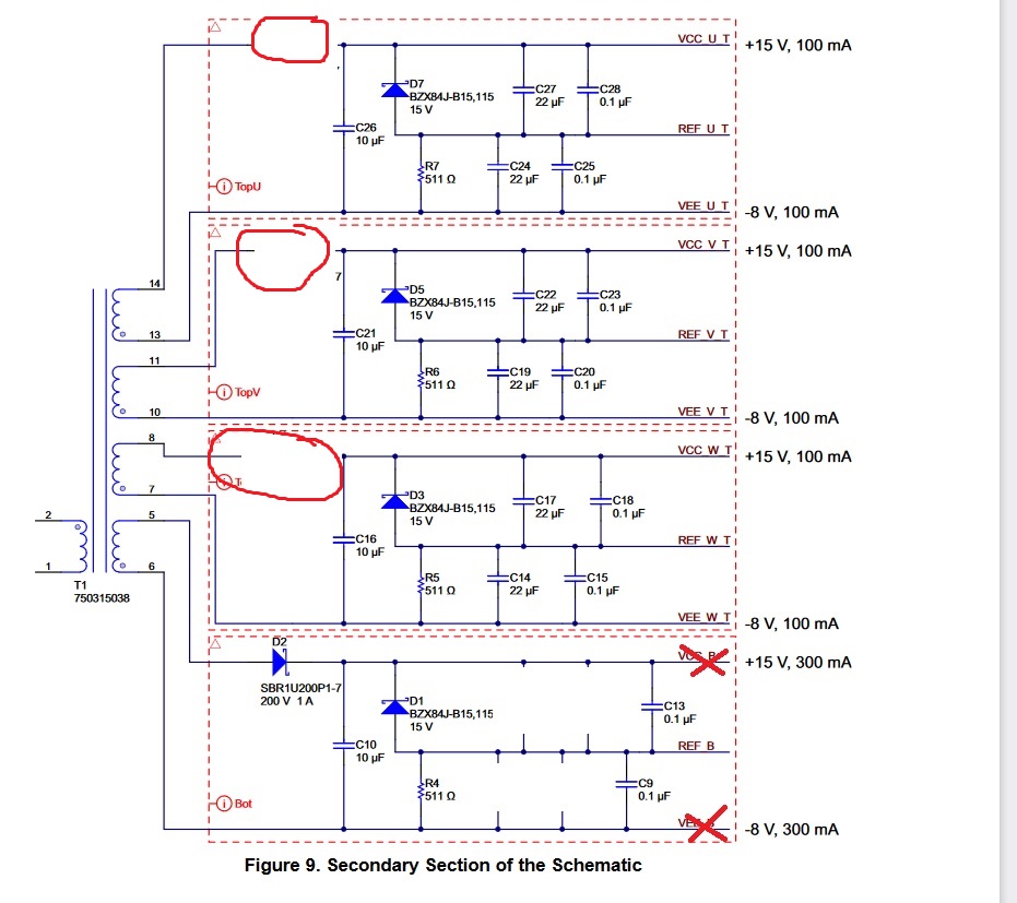
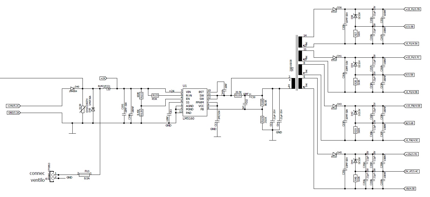
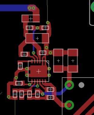
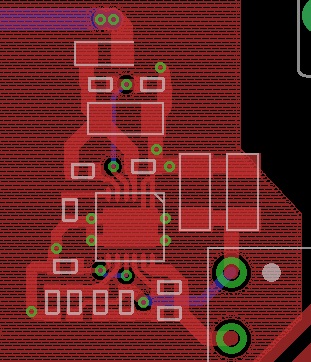
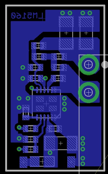
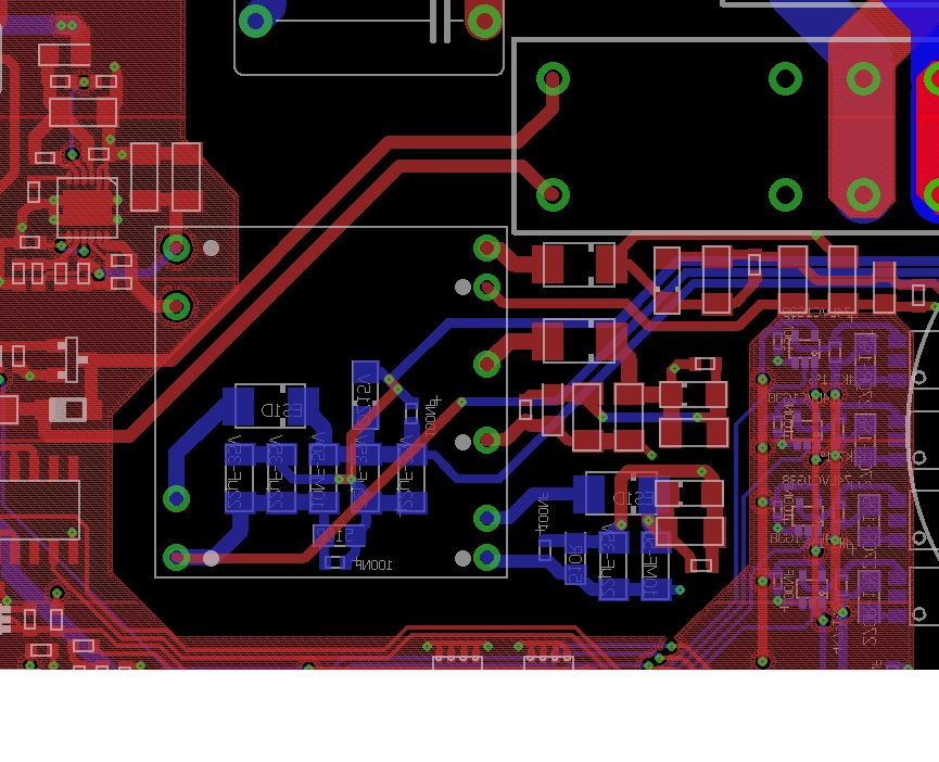
We implent the schematic of application note TIDU670a on our custom board.

So, the schematic is excatly the same then the evaluation board.

We have 24V on input Vin, then we produce 3v (+15V/-8V).

Our board is powerd by laboratory power 24V with switch.

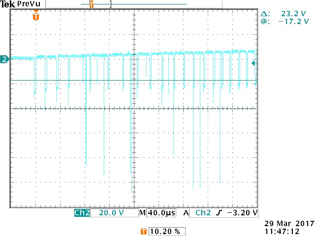
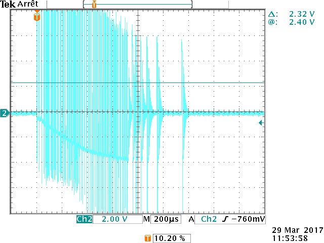
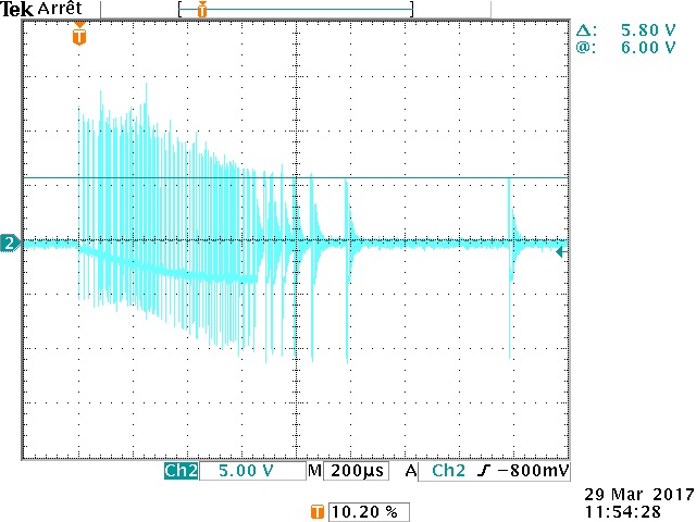
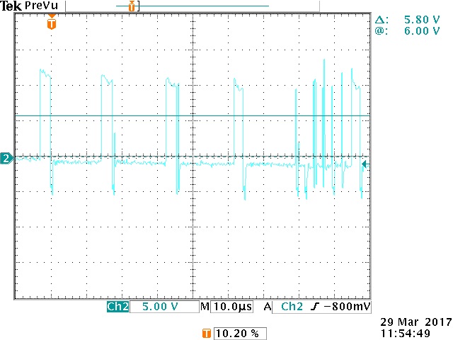
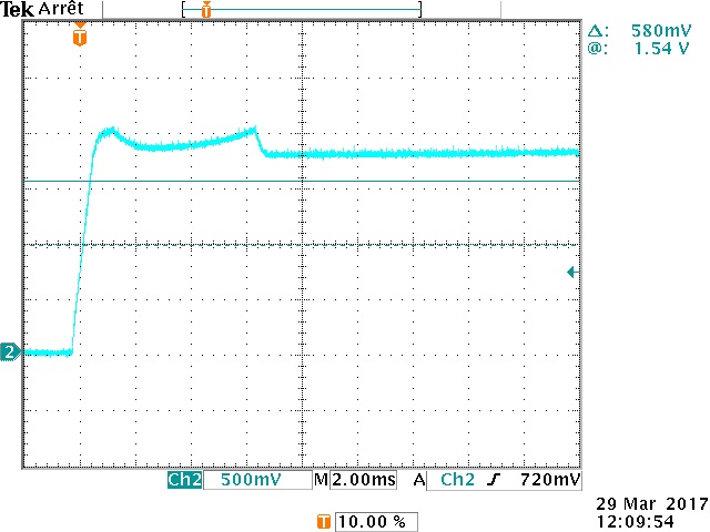
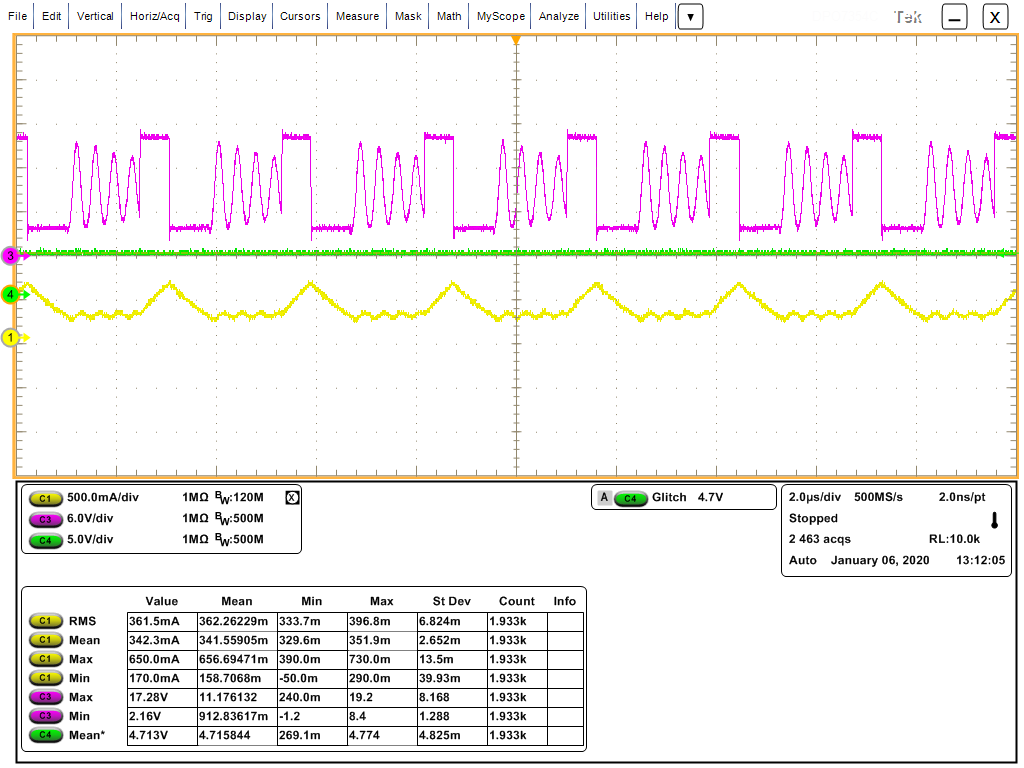
But sometime, when we power on the power supply, the output of the schematic (after the transfo) is 1.9V, not 23V (+15/-8)

This occurs some time, and to reproduce it, It switch Off on then switch on the power supply but I think before voltage imput fall to 0.

The problem occurs each time.

To try to understand, I make the following test:

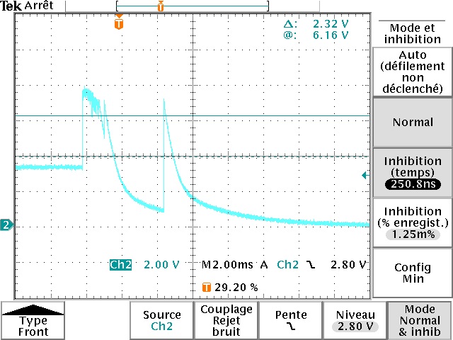
- Power on with Vin=24V => Output = 23V (+15/-8V)

- Down the power supply to 14V with the power supply potentiometer (this could take about 1, 2, 3s to down slowly to 14V) => output power is 1.9V => this is Ok, the LM5160 shutdown.

- Now, increase power supply up to 24V => the output stay to 1.9V, the LM5160 not start again to produce the power output 23V (15-98V).

I hope i'm clear, the question is: What could be the reasons makes the LM5160 not start properly?

Thank

  • A GIR,

    Let me restate to confirm we're on the same page:

    • Schematic is the same as TIDU670a
    • Layout is custom board
    • VIN = 24V, VOUT = 3x (+15/-8V), IOUT = ? 
    • 24VIN gives good startup (usually), lowering to 14V causes IC to shut down.
      • You say output power is 1.9V. Is this the output voltage on the primary or secondary of the transformer?
    • Increasing voltage from 14V to 24V does not cause the IC to start up again.

    Please check the SS pin voltage, FB pin voltage, and VCC pin voltage.

    If there is 1.9VOUT when the IC is off, is the IC still switching? Where is this voltage coming from?

    -Sam

  • Hello,


    Let me restate to confirm we're on the same page:

    Schematic is the same as TIDU670a
    => Yes it is exaclty the same

    Layout is custom board
    => Yes, it is a custom board

    VIN = 24V, VOUT = 3x (+15/-8V), IOUT =   
    VIn  = 24V, Vout = 1x(+15/-8V - 300mA)  + 3x(+15/-8V - 100mA).  

    on 3x(15/-8V - 100mA) there are only use to control IGBT gate driver with TLP5772 (high side)(one power on each TLP5772)

    The 1x (15V/-8V)-300mA is used to control the IGBT gate driver with 3 TLP5772 (Low side) + 3xAMC1304M25.

    During the test, the IGBT are not runing, then current consumption should be very low. There are only the 3 x AMC1304M25 which load about 6.5mA x 3 max according its datasheet.

    Then we can say the consumption is null on 3x(15/-8V -100mA) and max 20mA on 1x(15/-8V -300mA) 24VIN gives good startup (usually), lowering to 14V causes IC to shut down.

    You say output power is 1.9V. Is this the output voltage on the primary or secondary of the transformer?
    It is the outpur voltage on +15V/-8V -300mA

    Increasing voltage from 14V to 24V does not cause the IC to start up again.
    1) We discover first the problem because we power on the power supply 24V, and the get result of the AMC1304 was null. Then we check its power supply (15V) and it was about 1.9V.
    But this not occurs on each power on, this is random.
    2)Then we try to switch off and then switch On without long time of switch Off, and then the problem occurs each time.
    3)Then we try also to down the voltage 24V -> 14V (1.9V out), then increase to 24V =>out stay at 1.9V.
    I supposed the problem occurs on 1, 2 and 3 have the same root cause. But the normal case is the 1. The step 2 and 3 are only to try to reproduce the problem easily.

    Please check the SS pin voltage, FB pin voltage, and VCC pin voltage.

    Will come on the next message

  • Ch1 Yellow: Vin 24V

    Ch2 Blue: SS pin

    Ch3 Red: FB Pin

    Ch4 Green: Vcc pin

    Screen number 1 to 5 => with sometime Ok, sometime Nok. Whe can see when it is nok because we have no noise on SS Pin.

    If 24 Out is Ok, there are noise on SS Pin.

    Screen 6 : Only CH1 is Vout 24V (15V/-8V) when Nok: We can see a start and then a fall.

    Screen 7 to 11 diffeent start Ok and Nok

    Ch1 Yellow: Vin 24V

    Ch2 Blue: SW pin

    Ch3 Red: Vout 10V (Primary)

    Ch4 Green: Vcc pin

    Screen.zip

  • A GIR,

    Thank you for the waveforms. The SS and FB look very noisy. It makes sense that the noise correlates with normal operation because the switching may couple noise into the measurement but I'd like to see the measurement without the noise. Can you please set up a VOUT OK test again and measure just the SS pin with the tip-and-barrel method, disconnect other channels. If that noise is real, I need to see the layout because that noise can cause the device not to operate properly. If the noise is not real (just measurement noise) then I'd like to confirm some of the previous waveforms without the noise.

    -Sam

  • Hello,

    Please find the scope of SS signal with asked method.

    The noise seems ok?

    7268.TEK00001.TIF

  • A GIR,

    Yes that looks much better. If we assume that this method would clean up the other waveforms, we can conclude that VCC, SS, and FB look normal. FB looking normal means the device is regulating the primary output properly.

    Please confirm by sharing a scope shot of VPRI during OK and NOK conditions.

    I'm still curious about where the 1.9V is coming from. Is this 1.9V from the left-over charge when the load stops drawing power or is this a sustained 1.9V?

    Please share a scope shot showing the SW node during OK and NOK conditions.

    -Sam

  • Hello

    Thank a lt for your support and reactivity.

    Bellow the SW signal (Yellow) and Vpri (Blue) when Ouptut is Ok:

    1423.TEK00002.TIF

    Bellow, the same when output is not Ok. Scrennshot with different time base:

    1122.TEK00003.TIF

    TEK00004.TIF

    TEK00005.TIF

    Bellow the Output Transfo on the way 300mA, when work:

    7181.TEK00006.TIF

    And when not work (with different time base)

    1715.TEK00007.TIF

    TEK00008.TIF

    TEK00009.TIF

    Bellow the Vfb when work Ok:

    TEK00010.TIF

    And Vss when Work NOT OK

    TEK00011.TIF

    Please note that when we disconect the diode on all Transfo output (current load is null), never we reproduce the problem.

    If we connect only the way 300mA it is also ok. If we connect one of the 100mA way in more, problem can comes.

    Then the load on startup could make fail. But we could imagine always start with zero load!.. On our case, the load is very low (3 AMC1304 on the 300mA way, and gate driver on other, but at this step, not running, then consumption should be very low..)

    Regards

  • A GIR,

    It looks like the primary output is always regulated in OK and NOK conditions so the device is doing what it's supposed to be doing with the information it has from FB. So the waveforms showing SW for OK and NOK are reasonable for what the IC is seeing.

    Let's compare the transformer output:

    OK vs NOK

    7181.TEK00006.TIF OK

    1715.TEK00007.TIF NOK

    OK makes sense. SW goes high, VPRI = VIN-VOUT which is reflected to -33V on the transformer secondary. SW goes low, VPRI = -VOUT which is reflected to 25V on the transformer secondary.

    NOK makes less sense to me. SW goes high, we see the same behavior as OK. SW goes low, we only see about 2.5V reflected to the transformer secondary which means either VOUT_PRI must be around 1V (which we don't see from your waveforms) or there is some heavy load condition on a secondary output which brings this voltage down. Is it possible that the disabling/enabling causes your load to draw more power than in a regular condition? Maybe startup inrush current? You mention there is no issue if startup without diode (no load) which supports this theory.

    You said "But we could imagine always start with zero load!" If that is true, that may be the answer. Otherwise please share more information about your load.

    -Sam

  • Hello,

    "But we could imagine always start with zero load!"

    I made a mistake and miss "Not"! :

    "But we could NOT imagine always start with zero load!"

    I get VPri (Blue) and Secondary Diode rectifier current.

    When Ok:

    TEK00012.TIF

    TEK00013.TIF

    TEK00014.TIF

    And when NOK:

    TEK00015.TIF

    TEK00016.TIF

    The only difference with the Application note, is that we power 1xAMC1304 on the 300mA output, one on the first 100mA output and one other on the other 100mA output

    Edit:

    I just try to disconnect all AMC1304, the result is the same.

    The current consmption on secondary (300mA) is 40mA wherase no gate is yet used!. I don't explain this current condumption into the gate driver only!

    When I decrease the input power, the ouptut stay at 24V, but the current consumption on rectifier diode increase up to 80mA before shutdown when input is about 15.9V

    Note: the gate driver are TLP5772

  • Hello,

    I made the following scheme:

    With this, All it's Ok...!

    Now, just I replace C12 which is a 22µF on 15V way on 300mA output:

    In this case, I decrease slwoly the 24V input, then under a certain voltage (about 15.9V) we sse the the phenomen where secondary transfo is Ok on negative pulse, but the positive pulse not increase.

    From this, never we will recover the normal state when input will increase.

    If now I decrease the input voltgae fastly, then the secondary transfo is zero, no strange phenomene with two negative pulse and positive tranquated.

    To say in other word, the problem is on the shutdown, if output voltage decrease too slowly (due to capacity) then the "strange behavior" occurs.

  • A GIR,

    TEK00012.TIF - You said blue is VPRI. It looks like you're referring to the voltage across the primary winding, not the non-isolated buck output labeled Vpri. It looks like blue is measuring the voltage from SW (scope GND) to Vpri (scope signal). Please confirm because earlier you said:

    Bellow the SW signal (Yellow) and Vpri (Blue) when Ouptut is Ok: 

    1423.TEK00002.TIF

    But it looks like yellow is Vpri (buck output) and blue is SW. I thought it was a typo so I'd like to confirm.

    Comparing TEK00012.TIF to TEK00015.TIF shows that the blue waveform goes lower for the OK state (-40V? vs -20V?). If you're measuring as I described above, that means SW is going higher for the OK state. This can only happen if VIN is lower for the NOK state or if the BST capacitor is not charged fully. Are these waveforms taken with the same VIN? If so, check that C6 has about 7.5V across it.

    40mA at no load is probably caused by the zener/511ohm resistor rectifier. Confirm by removing one, or measure with a thermal camera. You can reduce this current by reducing the output voltage by changing the Vpri voltage by adjusting the RFBT and RFBB divider if desired. Or increase the zener diode zener voltage. Both of these solutions will slightly change the regulation voltage however.

    40mA through the secondary rectifying diode increasing to 80mA when VIN goes down is strange to me. I would expect the input current from the supply to go up since lower VIN means higher duty cycle which can cause worse regulation (leakage inductance) which increases the duty cycle more (figure 4). Check Vpri (buck regulated output) during this condition. Does Vpri go up when VIN goes down? That would cause the secondary outputs to go up which would dissipate more power in the zener/resistor regulator.

    Regarding your last message, check the primary winding voltage and the secondary winding voltage in these conditions and see if they match the turns ratio. Trace the circuit from the NOK signal back to the first OK signal you see. If VOUT_Secondary is bad, check V_PRIMARY (across the winding) and check Vpri (buck regulated output). Then check VIN (which should be OK). One of those will be OK and that will help us find the reason for the NOK voltage.

    Please also share the layout. That may be causing issues as well.

    -Sam

  • Hello,

    I'm so sorry, I made a mistake.

    I want mean:

    "I get Transfo Secondary (Blue) and Secondary Diode rectifier current."

  • Then, Following is the way to obtain the given graph bellow.

    - I reproduce the problem by increasing the input voltage from about 14V to 17V (Threshold is about 16V).

    - For each signal I trig on the first signal edge. I can't get all signal (Secondary/Primary) in the same time because the reference is not the same.

    -I suppose the trigger is always on the same moment, but I can't be sure.

    (I will try to do not make mistake on signal description! )

    - Blue = VSecondary (5 - 6)  - Green is current consumption at the output of scheme (Real current load of the way 300mA)

    We can see signal start, but after a certain time, problem occurs.

    Following is the same, but foccused time on the trigger:

    - bellow is the Primary voltage (2 - 1) = Vsw - Vpri:

    An other shoot:

    Focused on the startup trigger:

    - Bellow is In Yellow= Vsw, Blue Vpri:

    This is Vc6 (VBST - VSW) (Base time 2ms...)

    Vss (Base time 2ms)

    In fact, the problem occurs when input voltage increase so slowly. (> 50ms) But in our envirpnement, if we have noise,  we can be soumissed to voltage glitch then with filtering capacity, the voltage can evoluate and then cause this problem...

    :-(

  • A GIR,

    Please attach your schematic and layout. I know your said the schematic is the same as the reference design but I want to double check. And the layout can cause noise which may hurt performance.

    Picture 1: It looks like the device is regulating properly but the voltage is low. The top of the blue arc looks to settle around 10V but it should be 23V.

    Picture 2 shows the irregular pulses which may be due to the layout.

    Picture 3 looks like Vpri is regulating to about 3.9V (arc of the blue curve settles around 3.9V)

    Picture 4 confirms picture 3 comments

    Picture 5 shows some runt pulses which can be caused by layout.

    Picture 6 (Yellow=Vpri, Blue=Vsw?) shows Vpri regulating to ~6.3V. This should be 10.5V. Pictures from your post on Feb 5th show OK and NOK both have ~6.3V on Vpri. If this is okay, this is not the same schematic as the reference design.

    Picture 7 This looks odd. This voltage should be around 7.5V while the device is switching. Is the device switching during this scope shot?

    Picture 8 is interesting but I need to check if this is expected. It almost looks like the ground reference of the scope probe is drifting. Or VIN is collapsing.

    Is VIN good (steady DC, no big ripple or collapse) during these waveforms?

    -Sam

  • Hello

    Thank for your back.

    Picture 6: YOu are right, I might inverted signal ! sorry. For the voltage, I made new mesure this morning and measure 10.5V. I don't know why I measured 6.3V..

    Picture 7: I trig the scope on the first rising edge. It is the first signal rise when I increase input voltage from 14V to 17V.

    VIN is provided by laboratory power. Then I increase voltage frome 14V to 17V with the potentiometer.

    Bellow is the schematic:

    And then the Layout:

    With the Ground plane layer:

    My colleague which design the board said me all datasheet recomandation was not respected.

    So he design a new board to patch on the old board, He try to respect the datasheet recommandation.

    By this we will validate or not if the problem us due to a bad PCB.

    PLease, could you check if new PCB seems Ok for you?:

    We think we could test it on the next week.

    Regards,

  • A GIR,

    Thank you for sharing that information.

    Schematic: What is the part number for D36/D41/D43/D45?

    Layout: Please also share the secondary-side layout. The original primary-side layout looks okay except for the lack of ground plane on the top layer. The new layout looks better. You can rotate the top enable resistor to connect to VIN without a via and you may be able to rotate the RON resistor to do the same (with the EN trace going under the RON resistor)

    Picture 6: It is strange that you measured 6.3V and now 10.5V. This appears to be the issue. Please try to recreate this 6.3V and check the FB pin to see if it is as expected.

    Picture 7: I understand but is the device switching during the time when the boot voltage is falling? It's hard to tell due to the expanded x-scale.

    You say the power comes from a supply through a potentiometer. Please share the schematic for this. It should not be going through a potentiometer so I want to confirm what you mean.

    -Sam

  • Hello,

    The diodes are ES1D (On Semi), there are faster than the diodes indicated into the documentation.

    Find bellow the layout of the secondary side:

    When I said "potentiometer", it is this type of power, with integrated potentiometer to adjust output voltage and current limitation:

  • A GIR,

    The secondary-side layout looks good.

    Okay, I understand about the potentiometer now. That should be fine.

    Our next step is to find out what is happening with the Vpri. Sometimes it's 10.5V, sometimes it's 6.3V. Can you please confirm if this correlates with the issue?

    -Sam

  • Hello,

    Definitively, I don't measure again 6V on Vpri.. ..

    In blue, the Input power voltage (I make evoluate it with the power potentiometer..)

    In Yellow the VPri.

    I always get 10.5V, when output power (15V/-8V)  is OK or NOT

    Bellow, In blue, the Input power voltage

    In Yellow the Vsw. When Output Power is Ok, the Vsw is Square wave signal (Big Yellow rectangulaire on the screenshot due to the time resolution)

    When Output power is not work, Vsw is equal to Vpri => about 10.5V. If I zoom on the time base, we could see a try of square wave like showed on previous capture in other post.

    On this capture, we can see the first start is Ok, then I decrease the voltage under the 15V threshold where the chip goes into Shutdown state.

    After that, Output not restart when Input power increase again. I must decrease the Input Power near to 0 and then increase again to have a good work.

  • A GIR,

    Can you confirm that the FPWM pin on the LM5160 is connected to VCC? Please check with a scope. The device should be in forced PWM continuously switching but it looks like it's not.

    -Sam

  • A GIR,

    Also try placing a load on Vpri. Something like 50mA-100mA.

    -Sam

  • Hello,

    I measured on FPWM pin, I get 7,92V

    Also, I try to place a 120ohm between Vpri and GND, problem occurs also.

    We hop have the new PCB tomorrow.

    Regards

  • A GIR,

    Okay thank you for checking that. I will wait to hear the results from the new PCB.

    -Sam

  • Hello,

    I'm back to you after try our "PCB patch".

    We always get problem with the patch.

    So I compare the RFB1 and RFB2 value given into datasheet and the application note we were used.

    On the application note, RFB are about 86K and 20k where into datasheet, chapter 8.2.1.2.2FeedbackResistorDivider, RFB are 2k and 3k. Not atatch on the ratio value, because it depends of our wanted Vpri, but on the total resistor. About 100k in our case where the datasheet are about 5k. But it is written;

    Higher or lower values can be used as long as a ratio of the 3:2 is maintained.

    Then I try change Rfb from 86k/20k to 8.2k/2k. The ratio is aproximatively the same, but total resistor is 10 times less.

    With that, we resolve problem when Input voltage decrease under 16V and increase again. Output always restart correctly after many many try.

    But, We had anoter way to produce the problem. With ou laboratory power, we plug the power wire into them. Due to contact, we create some bounced like a Relay contact. Sometime, we get the problem where the output power not start like the previous way.

    And then, by this way, we always get problem. The probability is less, but always occurs.

    Then, we reduce again the Rfb resistor to 3.9K/1k (with PCB Patch), this is better, but we always get error.

    We try another modification: It is look like the LM5160 get problem to recover Normal mode from Standby mode, when EN/UVLO is between 0.35V and 1.24V.

    Then to reduce bounced due to power contact, we placed a 10µF capacity in parallele to the Ruv1.

    This perform again the result, but we always get error. Occurrence is very low, but we get again...

    So we have on our boad a power supervision based on the TPS386000. If input power decrease under 15.5V, the output goes loes.

    So, we removed Ruv1 and Ruv2 and connected the TPS386000 output to the LM5160 EN/VLO input.

    By this, we never get error, even after 10minutes of try!

    Then, with following modifications:

    - Patch PCB

    - Rfb decrease to 3.9K/930

    - EN/VLO controlled by TPS386000

    We get a correct behavior.

    We try on other prototype the only following modifications:

    - Rfb decrease to 3.9K/930

    - EN/VLO controlled by TPS386000

    -> No PCB Patch => We get error..

    So the PCB patch have some importance, but it is not the only needed solution.

    Then, we will try to make these 3 modifications on 5 Prototypes and test if we get error after many try and back here.

    I don't know what is your opinion about all these tests?

  • A GIR,

    I'm glad you have found ways to reduce the occurrence of the issue!

    Changing the resistor values makes me think the issue has something to do with the ripple emulation/injection circuitry (Rr, Cr, and Cac in TIDU670). Smaller resistor values means the injection circuitry has a smaller effect on FB. This makes sense because we've seen some switch waveforms which don't look perfectly stable. We've seen some runt pulses and unstable frequencies. If reducing the resistor values helped, I'm thinking we may be injecting too much into the FB node. You can try reducing the value of Cac or increasing the value of Rr to further adjust this subsystem.

    I think the ground plane on the patched newer layout helped. A solid GND plane is useful when dealing with issues like instability from the voltage on FB. It's optimal if the GND is moving as little as possible.

    -Sam

  • Hello,

    We increase Rr to 27k, 33k and 47k without success.

    We already try modify Cac (increase and decrease) without success.

    But we not try in the same time increase Rr and Decrease Cac.

    In any case, we observe problem on 2 prototype of 5 in our hand.

    On the first, problem occurs when we increase slowly the input voltage...

    On the second problem occurs when input voltage decrease and increaset fast, so the "Reset" signal with is controlled by the TPS386000 is so fast. I observe problem occurs when this time is < 150ms..

    On the first prototype, when it is blocked, we try to make another "Reset" on EN/UVLO pin, if this reset is fast, problem occurs. If the reset is long, Output is ok. When output is Ok, if we made another "Fast reset", problem occurs...

    In fact, It is like if we need a "proper long" reset time on EN/UVLO pin... ??

    Thank for your interset and very fast support. Congratulation and many thanks.

  • A GIR,

    I am going to step back and restate what we know so I can keep this organized in my head. From all of our analysis it sounds like the problem is that the isolated output is not regulated. But the primary output is regulated.

    The isolated output gets power when the SW node goes low. Primary winding voltage is Vpri - 0 = Vpri. This voltage multiplied by the turns ratio creates the voltage on the secondary which is rectified by the diodes and stored in the capacitors. If Vpri is regulated but the isolated output is not, that must mean SW is not switching low (or not switching low enough). A long reset will discharge Vpri which is why a long reset doesn't show the issue but a quick reset does.

    • SW not switching low will happen if Vpri is regulated and the device is in diode emulation mode. But we have confirmed that the device is in FPWM mode (please confirm).
    • SW will definitely switch low (and high) if the device needs to supply power to a load on Vpri. But we have tried adding a 50mA-100mA load to Vpri with no success (please confirm).
    • SW may not switch low if the ripple injection is injecting suboptimally, but this only makes sense if the device isn't in FPWM. But you have tried modifying that resistor and those capacitors, plus we're in FPWM. So this doesn't make sense either.
    • Or the isolated output load is too heavy. But we have tried no load and we still see the issue (please confirm).

    If you confirm all of the above, we need to check again if the SW node is switching during the issue. It must be switching if Vpri is regulated but we will need to confirm.

    Thank you too for your patience. We will get to the bottom of this :)

    -Sam

  • Hello

    • SW not switching low will happen if Vpri is regulated and the device is in diode emulation mode. But we have confirmed that the device is in FPWM mode (please confirm).

    Sorry, but I don't know how check if the device is in FPWM mode?

    • SW will definitely switch low (and high) if the device needs to supply power to a load on Vpri. But we have tried adding a 50mA-100mA load to Vpri with no success (please confirm)

    We tried with our load, without load, with only resistive load of 50mA. The result is the same

    • Or the isolated output load is too heavy. But we have tried no load and we still see the issue (please confirm).: Yes, the load has no influence on the problem.

    I make some other observation:

    - We perform the PCB,

    -We reduce Resistor on FB

    - We link the EN/UVLO input to ou TPS386000 controller.

    After that, when we increase input voltage slowly, problem occurs. With the scope, when problem occurs, an we observe the output signal of the TPS386000 linked to the EN/UVLO, we can see the 0V which is ok.

    When our trigger level voltage is reached (17V), the TPS386000 output goes High. THe LM5160 start.. but only during 1ms, because the TPS386000 output goes low again to return high after 4 or 5ms....

    The TPS386000 is open collector. A pullup resistor of 4.7K is present..

    But how interact the 20µA of EN/UVLo hysteresis on this?...

    We can see that when we link the TPS386000 out to LM5160 EN/UVLO, the signal has glith which lead to LM5160 output problem.

    If we have not glith on EN/UVLO, output is ok.

    THen definitely, I think we must have a propoer signal on EN/UVLO input. We tought we have it with the TPS386000 but it is not the case. May be due to Open collector output.

    We will try to add a logical "YES" to drive the EN/UVLO with a logical output...

    In your side, maybe you can try to reproduce the problem: Place a switch between GND and EN/UVLO and try to switch on/Off fast.. by this, out output not start.

  • 1. Checking FPWM: Check the voltage on the FPWM pin. If it is around 7.5V, the device is set to FPWM mode. Also check the switch node. If the switch node only goes high and low, we're in FPWM. If the switch node goes high, low, and has a decaying sine wave, we're not in FPWM (see purple waveform for example of not-FPWM operation).

    2. Adding load to Vpri: Try connecting an e-load or a potentiometer to the output and draw 100mA and 200mA. Maybe 50mA isn't enough.

    3. Isolated load too heavy: Okay this is not the problem, then.

    Regarding the TPS38600:

    A. "THe LM5160 start.. but only during 1ms, because the TPS386000 output goes low again to return high after 4 or 5ms...." Please share the schematic showing this connection. If you have a pullup resistor from TPS38600 connecting to the resistor divider on EN, I don't understand how it would turn on, then off, then on unless the TPS38600 is pulling it down again. I don't think the LM5160 EN hysteresis would cause this. We should focus on what is causing this issue because it sounds like avoiding this glitch can solve the issue.

    -Sam

  • Hello

    I'm so sorry for the late, I was in vacation and then, I switch to other emergency project.

    Then I back on this problem.

    Definitely, I think the problem come from the sensibility of the input EN which seem not accept some signal perturbation on its input.

    I think you could try to reproduce, just make a pulse à 1ms, then wait 1ms and then rise up definitely => Output not increase.

    So we link this innput to the output of TPS386000 but with some time filter.

    Please find the link to doxnload the schematic (Since forum updated, I can't access to the "Full editor" and can't add attached document!)

    If you can share this scheme, this could be great because the following link will disepears..

    https://www.dropbox.com/s/fw95ff0tmsob6ly/Scheme.png?dl=0

    The Signal PFD\ is the output of the TPS386000..

  • A GIR,

    This thread will lock soon since it has been open for a long time. Please post another question for additional help on this issue so we don't get locked out.

    Thanks,

    -Sam