This thread has been locked.

If you have a related question, please click the "Ask a related question" button in the top right corner. The newly created question will be automatically linked to this question.

TLV840: VOL specification

Genius 17315 points
Part Number: TLV840

Hello,

I have a question about V_OL specification of TLV840.

Usually Reset IC has to keep LOW signal during all VDD range less than V_IT+/-.
For example, when using Vth=2.8V, it has to keep LOW output from around 0V to 2.8V (I know it actually has V_POR).

So From this specification table, to keep VOL under 300mV from all 0 ~ 2.8V range, I think I_out(sink) have to be less than 15us from this table.
So I don’t think VDD=1.5V case and VDD=3.3V canse don’t have so much meaning.

For example using 10Kohm of pull-up for Vth=3.4V device, the sink current is


When VDD =3.3V, 3.3V/10KOhm = 330uA < 2mA. It's OK.

When VDD = 3.29V, 3.29V/10Kohm = 329uA < 500uA, It's OK.

When VDD = 1.49V, 1.49V/10Kohm = 149uA > 15uA, It's not OK. The reset output may be over 300mV from this specification table.

 
From this thought, if the user want to keep under 300mV from 0V to Vth, they have to use under 15uA condition from 0.7V to 1.49999V range.
Does this my understanding correct?

I feel this specification is a little bit strange.

Regards,
Oba


  • Hi Oba-san,

    I think your understanding of the sink current may not be correct.  The VOL spec is defined by saying that for VDD = 0.7V, 0.8V < VIT- < 1.5V, and with 15uA of sink current going into the pin, the voltage should not be higher than 300mV for those conditions.   With those conditions, here is the calculation of the resistor that one will need on their application to meet the entire VDD range.  Keep in mind that the lowest VDD is the worst case condition:

    (VDD - VOL) / Isink = (0.7V - 0.3V) / 15uA = 26.67kohms.

    Therefore, if the customer wants to ensure that the VOL spec is met across the entire VDD range, the best option is to use a resistor that is greater than 26.67kohms.

    I hope this clarifies your understanding of VOL and if you have further questions, please feel free to chime in.  

    Ben

  • Hello Ben,

    Thank you very much for your reply. 

    Sorry, I missed to subtracting 300mV .
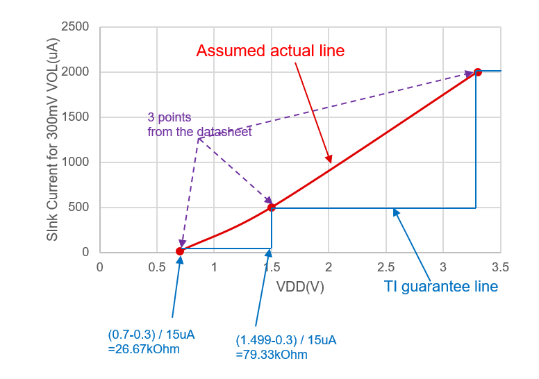
    Anyway, the below figure is my thought from the specification table.
    I plotted “VDD” vs “Sink current at 300mV VOL”.


    I believe that TLV840 actually has characteristic like RED line in the graph.
    But we specifies only 3 VDD points, 0.7V, 1.5V and 3.3V.
    The datasheet also doesn’t have typical characteristic graph of it like the RED line.

    So, to be safe, users have to think TI only guarantee like the BLUE line in the graph.
    This is the background of my question.

    Regards,
    Oba

  • Hi Oba-san,

    I think you have the right idea.  The current spec in the datasheet is just a test condition, as Shridhar mentioned in his email.  If the customer uses a large enough resistor to drop most of the voltage across the pull-up resistor, then VOL will be able to meet its spec.  

    One thing to note, the test currents that are being applied to the different VOL conditions is increasing with VDD because the higher the VDD voltage the stronger the devices internally are being turned on (VGS-VT).  This allows the internal FET (i.e. open drain device) to be turned on harder (lower RDSon resistance of the open drain device) and allowing more current to pass through the device and still meet the 0.3V max spec. 

    I hope my explanation answers your questions.

    Ben