This thread has been locked.

If you have a related question, please click the "Ask a related question" button in the top right corner. The newly created question will be automatically linked to this question.

TPS2834: Follow up to issues " TPS2834: Low side of MOSFET driver not operating at all when in synchronous mode and using in full bridge configuration. External modification had to be performed in order to get this working."

Part Number: TPS2834
Other Parts Discussed in Thread: TPS2830, LM5104,

Hello,

Following on from my previous post: 

Upon extensive further testing, we found that at higher operating frequencies (<100kHz), the pulling down of the bridge via a resistor was not suitable and we ended up with the same issue as originally described (low side MOSFET not switching on due to bridge voltage not going low enough). 

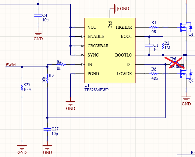
An additional solution that we have thought about is controlling the DT pin based on a delayed signal going to the input pin. In the schematics below I show how we propose that this would be done (JP6 would be not fitted), the DT pin is receiving the same signal is a IN pin with a 100ns delay. 

Are there any issues with running the IC in the proposed configuration? anything else that we would need to consider? 

Are there any other MOSFET drivers based on technology as the TPS2830 or TPS2834? our operation criteria leads us to stay away from CMOS technology whenever possible hence why other MOSFET drivers such as the LM5104 cannot be used.  

Thank you in advance for your response.

  • Hello Adam,

    You mentioned a schematic attached with your proposal but I did not see a file attached or the schematic diagram in your post.

    Can you add the schematic so we can review and comment on your proposed circuit.

    Regards,

  • Apologies about that, please find attached an image of the schematic

  • Hello Adam,

    Thank you for the schematic. After reviewing the datasheet it looks like you can accomplish what you desire by your proposed circuit. From the datasheet specs on the DT pin it looks like you need to guarantee a high of >2V and a low of <1V for the DT pin to recognized the transition allowing switching of the low side FET. You may need to adjust the time constant of the RC to achieve the timing that works best in your application.

    I would suggest testing the proposed configuration and see if the deadtime is what you are targeting in your design. The forum can benefit on your confirmation if this resolves your issues, so please confirm if this solves the issue in your design.

    Confirm if this addresses your questions or you can post additional questions on this thread.

    Regards,