


Other Parts Discussed in Thread: BQ24296M
Hello TI experts,
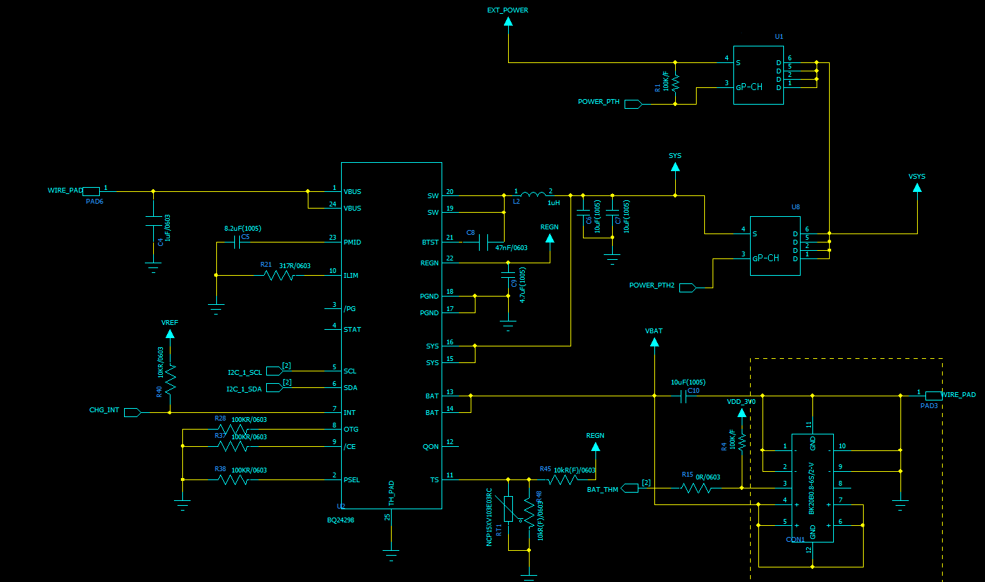
My customer consider BQ24298 for their product, so please review the schematic below.
and let me know if there are something to modify.
and here are few questions;
1. what is the maximum output current of SW pin? (pin19/pin20 -> marked as SYS voltage), we found I_SYS=3.5A in table 7.3. please check it right or not.
2. what is the recommended voltage for VREF voltage? actually we use 3.0V for IO of MCU. is it okay to use 3.0V for VREF?
3. about \QON pin, we understood that we can turn on BATFET by adapter or I2C communication or H->L transition on \QON pin.
then can we don't use \QON pin? if we don't use it, can we leave this in as floating? or connect to GND/VREF?
4. about U1 and U8 FET, sometimes we need very large current over 7A for the device so we want to bypass the adapter power directly to VSYS pin for device. of course these 2 FETs are controlled by GPIO, POWER_PTH/POWER_PTH2. please check this concept is right or not.
please check these issues. Thanks.
Best regards,
Chase
