This thread has been locked.

If you have a related question, please click the "Ask a related question" button in the top right corner. The newly created question will be automatically linked to this question.

BQ25790: False VSYS_SHORT fault.

Part Number: BQ25790
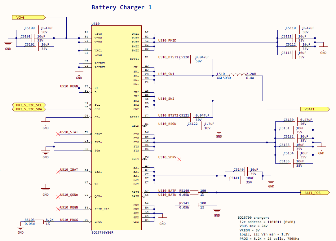
Other Parts Discussed in Thread: , BQ25792

New boards - 9 of 10 devices working fine with battery not connected (VSYS = 7.3V). 1 device reports VSYS_SHORT. Disabled charge, cleared EN_HIZ and fault repeats.

VSYS is not shorted and can be raised to 7.5V from external source with < 10mA. Total VSYS capacitance is 50 uF.

Input is 12V. Battery is not connected.

What else should I check?

Registers...

0000: 12
0001: 03
0002: 48
0003: 00
0004: C8
0005: 6C
0006: 01
0007: 2C
0008: 01
0009: 05
000A: 63
000B: 00
000C: DC
000D: 4B
000E: 3D
000F: 86
0010: 00
0011: 40
0012: 00
0013: 21
0014: 16
0015: AA
0016: C0
0017: 7A
0018: 54
0019: 00
001A: 32
001B: 0F
001C: 0A
001D: 00
001E: 00
001F: 10
0020: 00
0021: 00
0022: 80
0023: 00
0024: 10
0025: 01
0026: 00
0027: 80

  • Hi Jim,

    On your schematic, I see 0.47uF capacitors filtering caps on SYS and PMID.  Recommended value is 0.1uF because we found that high frequency switching noise could cause abnormal operation like SYS short.  How are those 0.47uF and the remaining capacitors on SYS and PMID laid out on your board?  On the EVM, the 0.1uF capacitors must be as close as possible to the SYS, PMID and GND pins. The BQ25790EVM user's guide shows our recommended board layout. 

    You also have ILIM_HIZ tied to REGN.  I can't find in the datasheet where it says that is allowed.  Your registers are reporting IINDPM=3A so apparently there is no issue with that.

    Your fault registers are reporting IINDPM active as well as VSYS Short fault.  For IINDPM to have been active, the load at SYS must have been very high at some point, and could be simply be the discharged capacitors at SYS.

    Also, as a side note, with TS pin ground, the charger will not be able to charge a battery unless TS feature is disabled via the I2C register. 

    Regards,

    Jeff

  • Thanks for the quick reply, Jeff. I've attached a view of the layout. The 0.47uF cap is circled in blue.

    Grounding TS was intentional - I wanted to prevent charging at startup until the microcontroller is running, so it sets the IGNORE_TS bit when it's ready.

    I will try changing the 0.47uF cap. I don't remember why I used that value.

    ILIM_HIZ was tied to REGN just for layout. I'm not using microvias, so some pins are not accessible. I did verify that it worked on the eval board, and I don't need the pin function, since the microcontroller is always setting up for charge.

  • I removed the 0.47uF but that had no effect.

    I connected a battery and enabled charge. CHG_STAT = 3 (fast charge), but the converter is not switching.

    Registers when it says its charging, but isn't.

    0000: 12
    0001: 03
    0002: 48
    0003: 01
    0004: CC
    0005: 38
    0006: 01
    0007: 2C
    0008: 01
    0009: 05
    000A: 63
    000B: 00
    000C: DC
    000D: 4B
    000E: 3D
    000F: A2
    0010: 00
    0011: 40
    0012: 00
    0013: 21
    0014: 16
    0015: AA
    0016: C0
    0017: 7A
    0018: 55
    0019: 01
    001A: 2C
    001B: 0F
    001C: 6A
    001D: 01
    001E: 00
    001F: 00
    0020: 00
    0021: 00
    0022: 00
    0023: 00
    0024: 00
    0025: 00
    0026: 00
    0027: 00
    0028: 00
    0029: 00
    002A: 00
    002B: 00
    002C: 00
    002D: 00
    002E: B8
    002F: 00
    0030: 00
    0031: 00
    0032: 01
    0033: 00
    0034: 00
    0035: 31
    0036: 83
    0037: 31
    0038: 91
    0039: 31
    003A: 9F
    003B: 1B
    003C: 4F
    003D: 1B
    003E: 44
    003F: 00
    0040: 00
    0041: 00
    0042: 2A
    0043: 0D
    0044: 93
    0045: 0D
    0046: 92
    0047: 00
    0048: 01

  • I added a 0.1uF cap from VSYS to GND on the backside of the board, directly under the BQ part. This also made no difference.

  • Jim,

    The 0.1uF capacitors are too far away from the IC to filter high frequency switching noise.  So, I can't rule out that layout as the issue.  Furthermore, the only layout we have tested is the BQ25790EVM layout with the SYS and PMID capacitors as close as possible to the IC.

    The charge SYS_SHORT feature is explained below:

    When the SYS voltage falls below 2.2 V, the charger immediately enters the PFM operation, to limit the output current to approximately 1A or less (regardless of the DIS_VSYS_SHORT bit setting). If the hiccup mode for SYS short is enabled by setting DIS_VSYS_SHORT = 0, the charger shuts down when the SYS voltage drops below 2.2 V longer than 10ms. After waiting for 500 ms, the charger attempts to restart the converter. After 10 ms of converter operation, if the SYS voltage is still lower than 2.2 V, the charger shuts down the converter for another 500 ms and the cycle repeats. After 90 s from the first short detection, if the converter shuts down for 7 times, the charger latches off the converter by setting the EN_HIZ bit to 1. If the VSYS_SHORT_MASK is low, the device also asserts an INT pulse is asserted to alert the host, the VSYS_SHORT_FLAG fault register gets set. The latch off is cleared when EN_HIZ bit is set to 0. If the system voltage is still lower than 2.2 V when the host clears the latch off, the charger enters the hiccup protection again. If the hiccup mode for system short is disabled by setting DIS_VSYS_SHORT = 1, the converter continues running in forced PFM operation when the SYS voltage is lower than 2.2 V. After 10 ms deglitch time, an INT pulse is asserted to alert the host if VSYS_SHORT_MASK is low, the VSYS_SHORT_STAT and VSYS_SHORT_FLAG fault registers get set.

    Are you certain that you input current limit setting and input power is high enough for the load on SYS at start up (keeping in mind that discharged capacitors look like shorts to GND)?  I can look at scope plots if you think it will help.  I would need to see VBUS, IBUS, SYS and ISYS if possible.

    Regards,

    Jeff

  • So VSYS_SHORT is not looking at current, but only voltage on VSYS?

    I connected an external 6V source to VSYS, applied power to VBUS and then removed the 6V. In this case, it still reports VSYS_SHORT.

    Some scope shots attached - sorry I only have 2 channels! In all shots, VBUS is red. I labeled the yellow.

    It looks like the SW1 FET isn't turning on fully, as it can't get SW1 above a few volts, even when I hold VSYS at 6V with an outside supply. Is this a bootstrap problem?

    VBUS + PMID:

    VBUS + SW1:

    VBUS + BTST1:

    VBUS + REGN:

    VBUS + VSYS:

    VBUS + SW1 (VSYS held at 6V initially, then external supply removed about 3 sec in):

  • Hi Jim,

    BTSTx should be roughly SWx + REGN.  So, only this board, BTST has a problem.

    Regards,

    Jeff

  • Comparing to a good circuit, I don't think BTST has a problem. BTST1 and SW1 look the same as the bad circuit up to the point where switching starts. After the initial 800ms or so, the good circuit starts switching, but the bad circuit does not. VSYS doesn't  get above 1V or so until switching starts, so it doesn't look like VSYS_SHORT could be detected that early. The problem seems to be that the bad BQ never switches. Even with a battery connected and VSYS up all the time, it doesn't switch to charge even though it says it's charging.

    VBUS + BTST1 (good)

    VBUS + SW1 (good)

    VBUS + VSYS (good)

  • Jim,

    The defective board is failing 7 times and then shutting off.  Is it possible there is a board solder problem?

    Regards,

    Jeff

  • Jeff,

    From your earlier post.. "if the converter shuts down for 7 times, the charger latches off the converter" so the 7 cycles is expected.

    But the converter never turns on at all. The bad and good BQ's both drive SW1 to ~1.5V for 800 msec at startup. Then the good BQ starts switching, while the bad BQ just turns off - not a single switching pulse on SW1.

    Since VSYS never went above 2.2V, it thinks it's shorted. But it didn't go high because the switcher never started. So it is a false short detect.

    The key question for you is what would cause the switcher to never operate, even though status registers say it should be (as when I connect the battery, VSYS is good, and the BQ says it's fast charging)?

    As for solder problems, I checked resistance and diode drops between all the relevant pins and they are all similar to those on the working charger. So definitely no shorts. It would be hard to have an open on the power pins anyway as there are 5 balls in parallel, but it's possible some single ball pin is open. Is there a pin that would cause this behavior if open?

    Thanks for your help! You're forcing me to look at everything and that's good.

    Jim

    EDIT: I should add that I have 2 identical chargers on a board. So I have just 5 boards made so far, with 10 chargers, and just this one not working. So I am comparing the good and bad chargers on the same board. The product is medical equipment and we have redundant batteries, each with its own charger.

  • Hi Jim,

    As I previously mentioned, it could be switching noise spikes that are not getting filtered by the placement of the capacitors.  We initially found similar faults until we placed the 0.1uF capacitors on SYS and PMID as close to IC as possible on the EVM.

    Can you scrape off solder etch and move those 0.1uF capacitors closer to the IC?

    Regards,

    Jeff

  • There isn't any GND on the top side. I did add a 0.1 cap on the bottom side directly under the chip on VSYS. I can add another for PMID and try it, but it still seems odd that there would be a switching noise issue when no switching has occurred.

    Can you confirm that you saw the same behavior (i.e. switcher never starts) before you moved the caps? Or did it see the VSYS short condition only after the switcher started?

    EDIT: Actually, GND is accessible on the top layer right in front of the chip where your eval board caps are. I will try to add caps there.

  • HI Jim,

    I don't remember the exact failure that we saw without those 0.1uF caps.  I just know that the device would not work correctly without them installed close to the chip.

    Regards,

    jeff

  • Jeff,

    I added 0.1 caps on VSYS and PMID next to the IC. I'm almost certain it worked the first time I powered it, but now it's back to failure. The SW1 waverform looks exactly the same as before.

  • Jeff,

    I have the eval board for both BQ25790 and BQ25792. I see that you made the cap paths much shorter on the 790 board than on the 792 board (~10mm). Were there problems with the 792 eval board? I will be moving those caps on my next layout rev, and I would like to know how your two layouts compare.

    Certainly the 790 layout is the ideal, but I'm wondering how close to that I need to be. I kept the SW1 and SW2 paths on the top layer and those have to go underground to duplicate your 790 cap locations.

  • Hi Jim,

    The 790 layout pic above is correct.  It is the final board layout.  When we first got back silicon we didn't install the 0.1uF capacitors and saw various false faults.

    The 792 layout above is the pre-release EVM.  Even on that EVM, in order to prevent the false faults, i had to flip those 2 0.1uF capacitors 180 degrees and run a small wire down the middle ground pin.  The final EVM layout, updated in the latest EVM user's guide online, is different as shown below:


    Regards,

    Jeff

  • OK. I think my added caps are very close to that layout. I will do it ideally on the next layout.

    But 9 out of 10 work as is, and the bad one still doesn't work with the added caps, so I'm still doubting this is the problem.

    Were you able to find any explanation for the switcher never starting at all?

  • Hi Jim,

    The only faults that stop converter switching completely are SYS OVP and BAT OVP.  ILIM_HIZ pulled low or set too low or the IINDPM register set too low or the input voltage at VACx drooping below VINDPM can also stop full switching but even then you should see pulses to keep BTSTx cap charged.    Since your registers didn't report any faults, other than SYS Short, we can try to debug our way through the chip.  Keep in mind the fault registers clear after being read so you need to read after power up and before the final retry of the 7 pulses. 

    First we can compare the dc voltages REGN and BTSTx of a bad board and good board.   

    How much current is the chip pulling when you apply power, before it shuts down? If you put the bad charger in HiZ mode, how current is it pulling?  Can you compare both to one of the other good boards?

    BTW, as I mentioned previously, I don't think ILIM should be pulled up to REGN directly.  When you change your board, I recommend using the recommend resistor divider.  I will check with design to confirm whether or not it is okay to tie REGN to ILIM_HIZ.  If so, you populate a 0 ohm resistor later.

    Regards,

    Jeff

  • Jeff,

    I will do the measurements you suggest shortly. I'm glad you mentioned reading registers before the 7 cycles are up. I haven't done that yet.

    I originally did the layout for the 792, since the QFN was easier to work with. When it was time to order boards, there were no 792's available so I switched to the 790. I was concerned that the 792 might not last, but now I see lots of those in stock and few 790's. The BGA works better thermally and actually runs cooler on my board than on the eval board since I have more layers to work with.

    The ILIM_HIZ to REGN was only done for layout. I can separate it from REGN on a new layout, as long as it is still connected to D+/D-, which should be OK, I think.

  • REGN = 5.015 on bad charger, 5.003 on good charger. Very stable.

    BTSTx = 5.0 on bad charger, since it's not pumping, 8.5-8.7 on good charger.

    Here's the register dump immediately after VBUS on - within that first 800 msec on time.

    VSYS_SHORT is flagged from the start. Reg 0x20 has both VAC OVP flags set.

    0000: 12
    0001: 03
    0002: 48
    0003: 00
    0004: C8
    0005: 70
    0006: 01
    0007: 2C
    0008: C3
    0009: 05
    000A: 63
    000B: 00
    000C: DC
    000D: 4B
    000E: 3D
    000F: A2
    0010: B5
    0011: 40
    0012: 00
    0013: 21
    0014: 16
    0015: AA
    0016: C0
    0017: 7A
    0018: 54
    0019: 01
    001A: 2C
    001B: 2F
    001C: 0A
    001D: 00
    001E: 00
    001F: 10
    0020: 03
    0021: 00
    0022: AF
    0023: 12
    0024: 50
    0025: 11
    0026: 03
    0027: 80
    0028: 00
    0029: 00
    002A: 00
    002B: 00
    002C: 00
    002D: 00
    002E: 30
    002F: 00
    0030: 00
    0031: 00
    0032: 00
    0033: 00
    0034: 00
    0035: 31
    0036: 22
    0037: 00
    0038: 00
    0039: 00
    003A: 00
    003B: 00
    003C: 00
    003D: 00
    003E: 00
    003F: 00
    0040: 00
    0041: 00
    0042: 00
    0043: 00
    0044: 00
    0045: 00
    0046: 00
    0047: 00
    0048: 01

    Current traces below are for two chargers, since I can't separate their VBUS inputs. Traces are 40mA/div (10 ohm series R). There is a system load increase 5 sec out. At that point, total input current ~20mA. Very little difference between the boards.

    Bad charger + Good charger:

    Two good chargers:

  • Hi Jim,

    Your comment about VAC_VOP reminded me that the default VAC_OVP for 790 is 7V while 792 is 20V.  If you have any ringing at VBUS that hits 7V, the converter shuts off.  Could that be your issue?

    Regards,

    Jeff

  • Jeff,

    My VBUS is normally 12V. The first thing I do is zero VAC_OVP. But that only happens after the BQ shuts down.

    Seems like a catch-22, if the microcontroller has to change that OVP before it is powered.

    EDIT: Also.. 9 of 10 chargers work at 12V after I set VAC_OVP, but 1 doesn't recover.

  • Hi Jim,

    The BQ25790 VAC_OVP was lowered to 7V at the request of the main customers, who are cell phone manufacturers.  In cell phones, charging starts from a 5V adapter but can be negotiated higher.

    If you try to power from 5V, does the bad board work?

    Regards,

    Jeff

  • No.. I tried turning VBUS up slowly from 0 and it never started switching.

  • Jim,

    I'm not sure where to go from here. We can continue looking at quiescent current values to see if the IC is damaged.  If I had the IC, I would remove it from the board, reball it and install on a known working board, like the EVM, in order to see it if the issue follows the IC or the board. Or take a working IC from a working board and install on the failing board. You probably can't do that easily/inexpensively because of WCSP.  But, you could remove the failing board IC and install another IC.  You are welcome to submit the failing IC as a return but the return process is not fast.

    Regards,

    Jeff 

  • Thanks, Jeff.

    I will keep that option open. Certainly our CM can replace the part and I would ask them to X-ray first to check solder. I'm about to turn on the assembly of 20 more boards, so in a few weeks I'll have a larger population to test and then I may do the return process.

    For the next version of the board, I need to decide between the 790 and 792. The only reason I would change is that I can access all the pins on the QFN, so they can all be connected per the datasheet and to verify solder if there's a problem.

    I thought that the WCSP was better thermally, but the datasheet thermal numbers don't show that. It's hard to see how the small pads on the QFN can match the multiple balls of the WCSP. Do you have any comment on that question?

    We can close the thread, but I can't really say my issue is resolved yet.

    Jim

  • Jim,

    The QFN package is a new one that has better thermal performance that previous versions.  WCSP is still slightly better thermally but not much.

    Regards,

    Jeff

  • OK. If we decide to return the part, what's the procedure?

  • HI Jim,

    It depends on where you bought the ICs.  If you went through a distributor, then you have to return through them. If you bought direct from TI, then you follow the instructions at the link below:

    Regards,

    Jeff

  • I bought them direct from TI.

    I will mark this resolved. Thanks for all your help, Jeff.