This thread has been locked.

If you have a related question, please click the "Ask a related question" button in the top right corner. The newly created question will be automatically linked to this question.

TPS53355: TPS53355 VFB issue

Part Number: TPS53355

TI guys

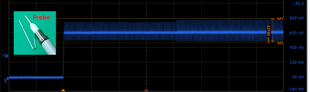
we meet a issue for TPS53355 design, refer to below pic for sch.  the snubber circuit R1871=0,C2645=2.2nF.

we test the waveform on the VFB pin(Point C) with and without snubber(remove R1871) separately.

we find the snubber will affect the VFB waveform largely. 

Is it normal ? and how the snubber affect VFB ?

TKs.

  •  (TK) 

    A Switch Node Snubber provides a low-impedance path to ground for high-frequency currents charging the switching node, especially resonant ringing of the capacitance of the switch node with the parasitic inductance of the charging path.  That low-impedance path can carry a large amount of current., especially with a "Zero Ohm" (typically 20-50mOhms) resistor in series - Form example, charging 2.2nF of capacitance to 12V in 4ns drives more than 6A of current into ground.

    This high current pulse into ground can create voltage gradients across the ground plane, which add noise spikes to the measurements, especially if the return path from the Snubber's ground to the input capacitor bypass ground and low-side FET source pass the ground reference for the feedback divider.

    If two or more probes are used, it is also possible that the high-frequency spikes on FB are measurement artifacts.  The grounds of an oscilloscope are generally shorted together, any differential voltage between probe ground connections forced by the PCB are created cross the ground return wires to the oscilloscope and then gained up but the amplifier that is compensating for the 10:1 passive probe's divider ratio.  At 60mV 200MHz noise spike between grounds becomes a 600mV noise on their respective signals.

    Recommendations:

    1) Check Probe measurements.

    Make sure there is only 1 ground clip location for measurement

    Make sure the ground clop location for the measurement  is as close to the IC's AGND input as possible.

    You can even place a probe on the AGND pin to check how much differential ground noise you are picking up if you are measuring from a different ground point.

    2) Check Snubber return current path

    Both to Cin and to the source of the low-side FET (Thermal Pad / PGND)

    Make sure the snubber return-path does not force current between the AGND connection for the FB to AGND resistor.

    3) Increase Rsnubber to 1-Ohm

    To optimize the resistor value, you can measure the SW ringing frequency with and without the 2.2nF snubber capacitor and measure the change in frequency, then calculate the parasitic inductance and parasitic switch node capacitance, then set the snubber resistor as close as possible to the characteristic impedance oft the LC  resonance.

    Freq1 = 1 / [ 2 * pi * Sqrt (Lpara x Cpara) ] 

    Freq 2 = 1/ [ 2 * pi * Sqrt ( Lpara x { Cpara + Csnub } ) ]

    ( Freq 1 / Freq 2 ) ^2 = ( Cpara + Csnub )  / Cpara 

    The Ideal Snubber Resistor is Sqrt ( L para / (Cpara + Csnub ) 

  • Hi Peter James Miller

    Thank you for the detailed analysis, there are more informations about this issue below.

    1) Check Probe measurements.

    I test the VFB signal by the Keysight N2870A  probe (1:1 passive, 1MΩ input, 35M bandwidth) with ground spring, and only use one oscilloscope channel, and we re-test it by limit the bandwidth to 20M, it seems the case with the snubber still is abnormal.

    2) Check Snubber return current path

    the layout refer to below pic, i already mark out the snubber RC /DC output /DC input location, there is a via A that connect the top layer LL to the bottom layer snubber circuit, it looks workable. please help check if the layout will cause this issue.

    3) Increase Rsnubber to 1-Ohm

    I am planning to do this test with Rsnubber 1ohm later.

    i also test the LL with/without Rsnubber 0ohm, it seems the waveforms of  LL  are similar with/without snubber .


  • Thank you very much for sharing.  Looking at the switching node, we see a 170MHz switching node ringing.  With a 35MHz bandwidth probe, it's not surprising we do not see much shift going from 35MHz bandwidth to 20MHz bandwidth, though it's hard to infer much about the switching node from a 35MHz bandwidth limited measurement.

    There does not appear to be much frequency shift between with a snubber and without, which makes me question if the inductance from the single via pass-through is limiting the effectiveness of the snubber   WIth little improvement in the 170MHz ringing, the snubber may not be necessary, though I would recommend a higher-frequency probe is one is available.

    The layout looks pretty good, but I would recommend using the same oscilloscope probe to measure the ground voltage near the Vfb pin with and without the snubber, just in case there is an "Earth Ground" connection on the board somewhere that  is inducting a ground current through the oscilloscope  probe.

  • Hi Peter James Miller


    The TPS53355 output voltage is different when we use the different datecode TPS53355 chip,

    on the same board with snubber(R=0), the old one output always 0.9V, and the new one output always 0.85V, 

    is it normal ?  

  •  

    No, that is not normal.

    The regulated voltage at the FB pin should be 0.6V.  With your 10k resistor from FB to GND and 5k resistor from FB to VOUT, the converter should regulate to 0.9V regardless of the date code.

    1) Double check R609 and R614 to make sure they are 3k and 2k and not 2k and 2k, which would give a regulation voltage of 0.84V

    2) If the resistor values are correct, check the voltage at the FB pin, it should be 0.6V

    3) If the resistor values are correct and the FB pin is 0.6V with VOUT 0.85V, check C689 to make sure it isn't shorted out and conducting current into FB around R609 and R614.

  • I replaced the new datecode chip only, that meanings other components keep to the same.

    the VFB pin voltage as earlier posted picture show that has a large noise, the VFB noise on the the new and old datecode chip almost are same .

    but the output voltage is different (0.85V vs 0.9V),so it is very strange.  maybe the different datecode chip has some difference ?

  • Hi,  

    It is really strange the output change just because replaced a new datecode chip. Could you help try with another chip to check what's the output voltage?

    Anyway Peter can help follow up after the weekend.

  • we also use the new datecode for other power rails(5V,1.8V.etc.) that all work well, only the 0.9V power rail is incorrect

  •  

    It is very strange that a shift in the part is resulting in a low output voltage.

    While the Constant On-time (COT) control mode at the CORE of D-CAP can respond to noise, the valley control used in D-CAP typically produces a high output voltage, not a low output voltage, when responding to noise.

    If you measured the FB voltage and it is reporting 600mV average voltage and the output voltage is reporting 850mV, something is leaking current into the FB pin to create the error in the output voltage and we need to find the source of that current.

    If you swap one of the other TPS53355 converters use in the 5V or 1.8V rails with the one used in your 0.9V rail, does the error in output voltage follow the swapped device or the board location?

    How many boards have you built up with the new date code?