This thread has been locked.

If you have a related question, please click the "Ask a related question" button in the top right corner. The newly created question will be automatically linked to this question.

LMR23630: Switching Frequency between 50kHz and 80kHz, why is it not closer to 400kHz?

Part Number: LMR23630

24Vin / 3V3 out, load is maybe 100-200ma normally, but even with 1.6 amp load the switching frequency is still only 80kHz.

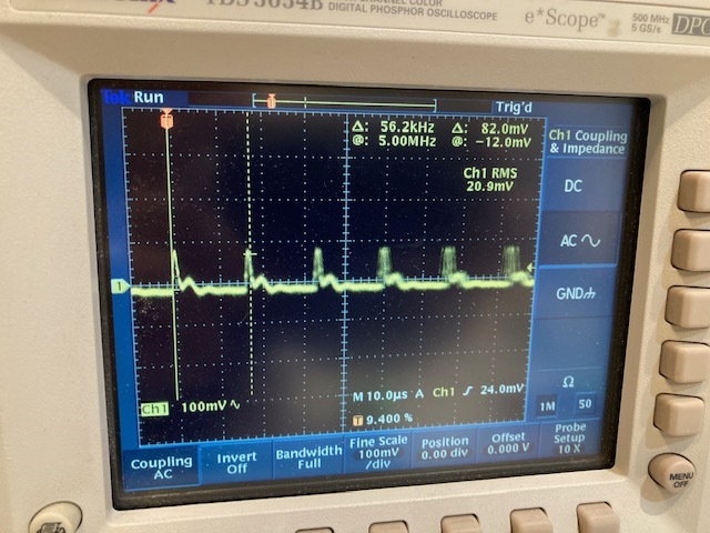
I am trying to understand is this is normal or if something is wrong?  The way I noticed it, was looking at the 3V3 ripple and saw ~ 60kHz spikes at ~ 100mV with maybe a couple hundred mA of 3V3 load current.

I sent the schematic and scope plots of the switch node to a customer care person last night, case #CS0418078, hopefully you can review the case and get back to me.  They referred me to you...

Thanks,

Jeff

  • Jeff,

    Please share the schematic and scope plots on this thread. I'm not sure how to access that case or where it is being taken care of.

    Have you witnessed the switch frequency at this frequency by probing the switch node?

    If not, the ripple may be caused by instability.

    -Sam

  • Hello,

    Yes I see these frequencies on the switch node as well.  I'm not sure how to attach the schematic / plots, I will try and reply to your email with the schematic and pictures.

    Thanks,

    Jeff

  • Hello,

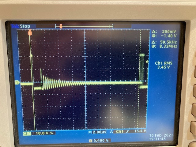
    Yes I see these frequencies on the switch node as well.  See the pictures below

    Thanks,

    Jeff

    Ripple with a 1.6 amp load

    Output Ripple with very light load

    Switch Node with very light load, maybe a few hundred mili amps

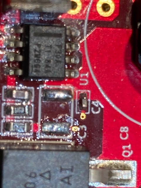
    The part on the board

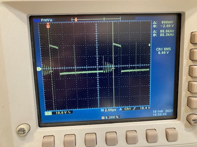
    Switch node with 1.6 amp resistive load.

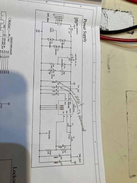
    Schematic, note I swapped out the .047uf boot cap with a .47uf cap to match the app note, and it did not make any difference.

    So all of the plots you see the boot cap is .47uf.

  • Jeff,

    The switch node at 1.6A looks to be the right duty cycle for 24VIN, 3.3VOUT. This makes me think the device thinks it's operating properly. I also see C4 is mounted far from the VIN and PGND pins and I don't see C5. This large input loop will introduce parasitic inductance which can cause excessive switch ringing and VIN noise. This might be enough noise to couple into the EN/SYNC pin to cause the device to think it's receiving a synchronization signal. This would cause the device self-referentially switch which could possibly drift down to the devices' minimum synchronizable frequency which, in this case would be ~88kHz. You can test this theory by adding a capacitor (a few uF) directly across the VIN/PGND pins. This should clean up the noise and should cause the device to default back to the internal 400kHz.

    If we require other theories, here are some other thoughts:

    The schematic is a little difficult to read but it looks alright. My only comment is to check the ESR on the output capacitors. We recommend ceramic capacitance on the output with the addition of a bulk cap if desired. The ESR may be causing some excessive ripple.

    Please share the layout as well.

    -Sam

  • Hi Jeff,

    I haven't heard back. Did this resolve the issue?

    Thanks,

    -Sam