This thread has been locked.

If you have a related question, please click the "Ask a related question" button in the top right corner. The newly created question will be automatically linked to this question.

TPS65130: TPS65130 +15V and -15V startup issue

Part Number: TPS65130

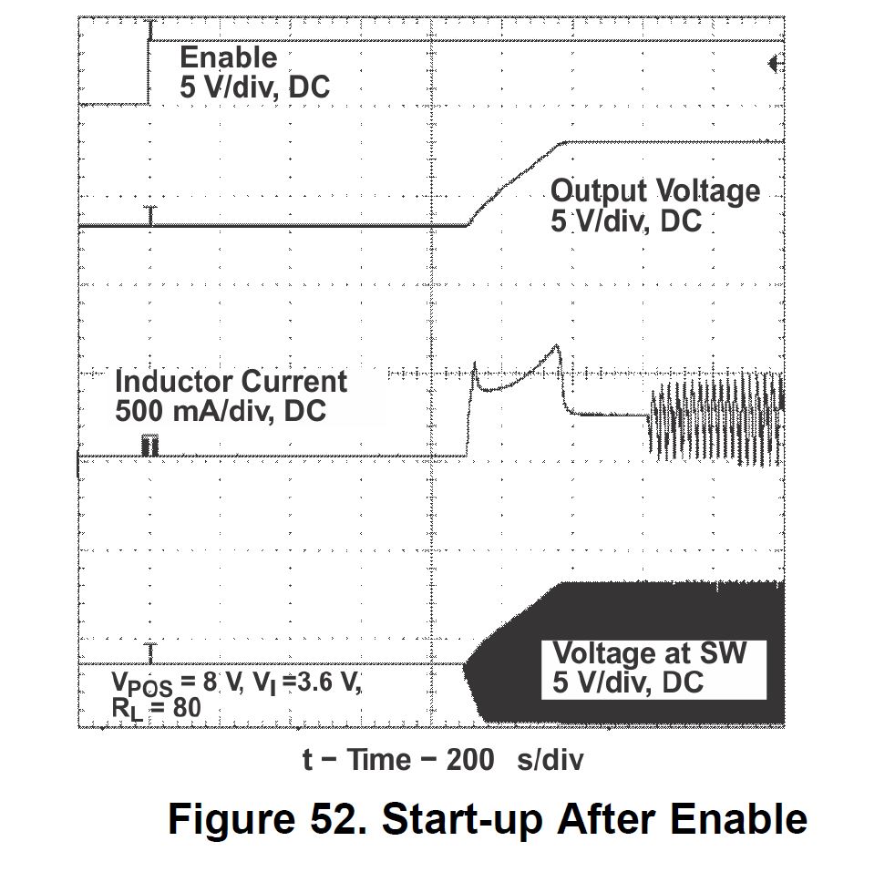
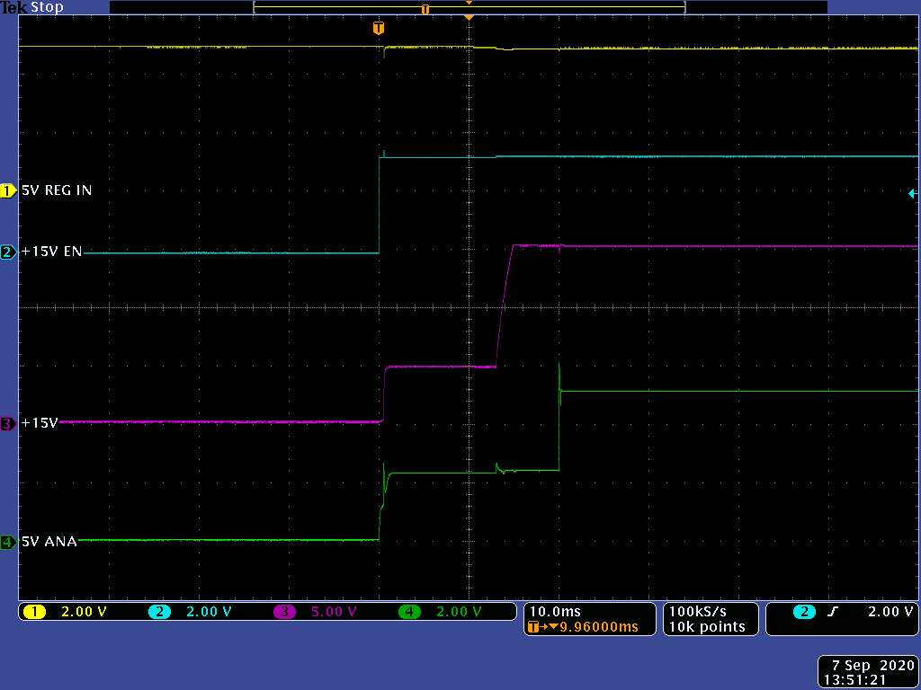
Hello, We have designed TPS65130 regulator circuit for +/-15V regulation. During power up we are seeing that -15V startup seems to be correct but +15V is not correct as we are seeing step from +5V after enable and after around 12ms +15V will be up. This is not the expected behavior and we need to solve this. Please can you guide /provide your suggestion as what could be causing this issue.
I have attached scope images for your reference. One is showing +/-15V startup and other showing 5V input to regulator, regulator enable, +15V and 5V LDO output connected to +15V output.
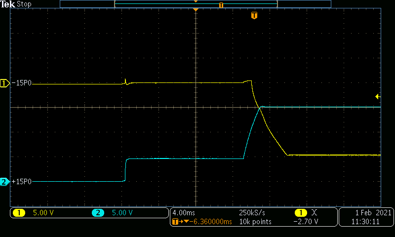
  • Hello,

    What you are seeing is actually expected because for boost (+15V), even before ENP signal is asserted, +15V will have input supply minus the diode drop appear at the output. Once ENP is asserted, boost converter starts switching and output ramps up to the set 15V.  That is the reason for the step in the boost output.

    Kind Regards,

    Liaqat

  • Hello Liaqat,

    Thanks for the reply. Actually in this design this should not be the case as we have FET to enable input voltage for the switching.

    The 5V on the +15V rail what we are seeing is after ENP is driven high. This is not expected and also from TP65130 datasheet waveform it should be smooth rise from 0V to set output voltage and not a step.

    Regards

    Roshan Dsouza

  • Hello Roshan,

    From the scope plots, I assumed  that there is no FET switch in series with input power in your design because of the long 5V step. In any case, even if there is FET switch in series with input supply, there will still be s step first of input supply minus a diode drop and than boost will start switching to achieve the final set voltage. In the datasheet figure, it appears that there was no FET in that measurement and boost output voltage was already at input supply minus the diode drop at the start of the scope trace. There is no indication in the datasheet plot that boost voltage is rising from 0V to boost set voltage. I believe it rising from initial step of input supply minus diode drop to final set voltage. Having said that, it does appear that the delay of step in your case is quite long. Can you please attach schematics of your design and I will review to see if can spot something.

    Kind Regards,

    Liaqat

  • Hello Liaqat,

    Thanks for the details. Yes the datasheet scope shot also does not show rise from 0V.

    I have attached my schematics for review.

  • Hello Roshan,

    As discussed earlier, the step at the boost output voltage will be there are at power up but it seems a bit longer in your application than I would normally expect. Reviewing the schematics, there are couple of things I noticed that could possibly be contributing to this longer time. The recommended values for compensations capacitors at CP and CN pins are 10nF and 4.7nF respectively. So you may want to change the network at these pins to match the typical application schematics of the datasheet. Calculated values for the feed-forward capacitors C73 and C74 from equations 11 and 12 in the datasheet comes closer to a standard value of 68pF so I would suggest to use this value. Recommended value in the datasheet for VREF filtering capacitor C57 is 220nF. Unless there are specific reasons for deviating, I would suggest to stick with the component values recommended in the typical application schematics in the datasheet.

    Kind Regards,

    Liaqat