Hi
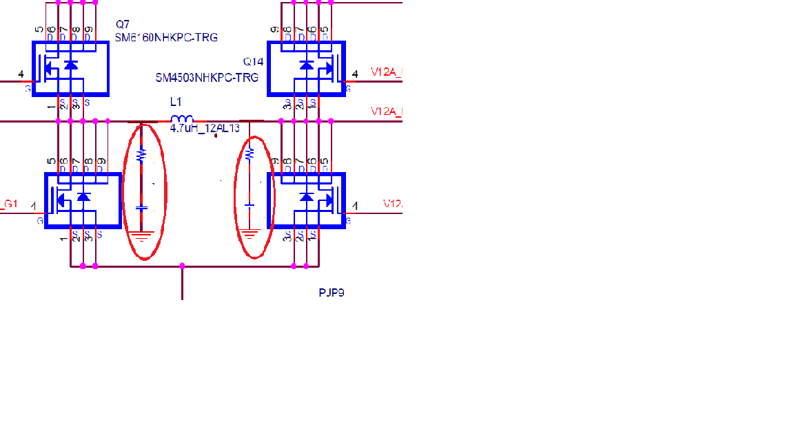
1.Could you please check the LM5176 schematic as below and any need to adjust
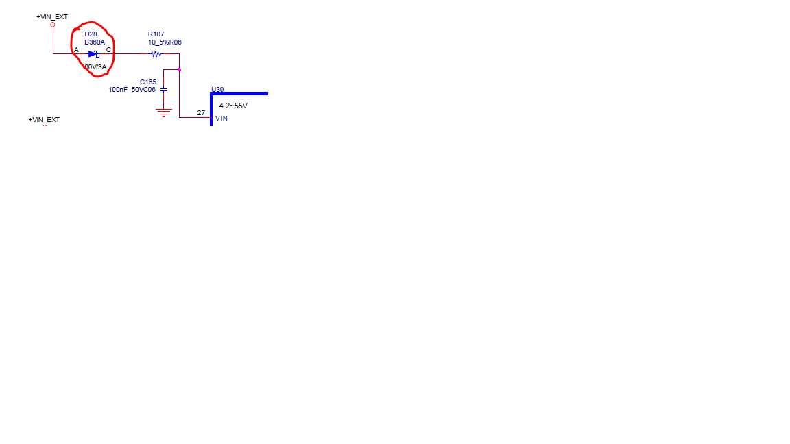
2.What is the function of Dvin? Can it be replaced by BAS316 250mA or can be removed
Hi
1.Could you please check the LM5176 schematic as below and any need to adjust
2.What is the function of Dvin? Can it be replaced by BAS316 250mA or can be removed