This thread has been locked.

If you have a related question, please click the "Ask a related question" button in the top right corner. The newly created question will be automatically linked to this question.

LMZM23600: Thermal Resistance to Ambient, Figure 81 on the datasheet

Genius 17295 points
Part Number: LMZM23600

Hello,

I have some questions for Figure 81 on the datasheet of LMZM23600.
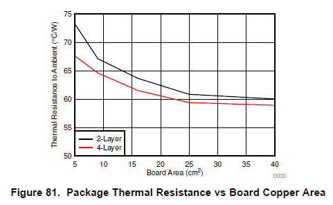
 

1.
Is the vertical axis of graph, “Thermal Resistance to Ambient(C/W)”, the same as R_Theta_JA except for the board size environment?
R_Theta_JA is specified as 45C/W on page 5.
I know the thermal resistance to ambient highly depends on the environment. And the board size is one of big factors
But I feel that the values on Figure 81 are a little bit difference from R_Theta_JA, 45C/W.
So I want to confirm what Figure 81 shows.


2.
I would like to confirm where is Tj in this device.
Does “Tj” mean silicon die temperature inside this module like other usual ICs?

Regards
Oba

  • Oba,

    1. Let me check on this and get back to you later today or tomorrow.

    2. Yes, TJ is the junction temperature of the silicon die.

    -Sam

  • Oba,

    The 45C/W is taken from a simulation using the JEDEC standard which is typically not accurate to a real-life test, especially for power ICs, especially for modules. The chart gives data tested on the bench so that is the data which should be used for thermal performance estimates.

    -Sam

  • Hello Sam,

    Thanks for your answer and sorry for my late response.

    I have some additional questions related to the below post.

    https://e2e.ti.com/support/power-management/f/196/t/758238

    Jimmy answered like the below.

    I would measure the temperature centered on the exposed inductor. During thermal characterization of this part I used an IR gun pointed at the exposed inductor to help create Figure 69.  

    Is Tj in Figure 69 actually temperature at the top of inductor?
    Or is it assumed Tj calculated from the temperature at the top of the inductor by using Psi_JT parameter?

    And Denislav answered “I believe the Psi_JT was measured in from the embedded die to the top of the laminate PCB.”

    I can’t understand where is “the top of the laminate PCB” for Psi_JT.
    Is it right under the inductance? I think it is impossible to measure it and it is impossible to know Tj.
    Could you please clarify where is the “TOP” in Psi_JT?

    Regards,

    Oba

  • Oba,

    The top is measured at the top of the PCB substrate where the IC is embedded. You are correct that the inductor is in the way. This top temperature can be measured if the inductor is rotated to stand on its edge and moved a bit to the side so it's still electrically connected but you can see the top. The results will be slightly better than when the inductor is in its original state but it will be a close estimate.

    -Sam

  • Hello Sam,

    Thanks for your reply.
    I understand where the top for Psi_JT.

    Then I am not still clear the below question
    Is Tj in Figure 69 actually Tj or the top of the inductor?

    >Jimmy answered like the below.

    >I would measure the temperature centered on the exposed inductor. During thermal characterization of this part I used an IR gun pointed at the exposed inductor to help create Figure 69.  

    >Is Tj in Figure 69 actually temperature at the top of inductor?

    Regards,
    Oba

  • Oba,

    Let me check with Jimmy and confirm

    -Sam

  • Hi Oba,

    Apologies I believe I might have linked the incorrect thermal resistance image in my previous E2E post.

    In my previous post I meant to reference Figure 82 (Package thermal resistance vs board copper area). I refer to Figure 82 as a quick guide for customers to use to quickly check if their board is big enough to prevent junction temperature from hitting 125degC. 

    If you are wondering how to calculate Tjunction temperature, I would take the IR thermal camera measurement right at the center of the exposed inductor. 

    The inductor is mounted right above a PCB substrate with the silicon embedded inside.

    For this package with a 3D mounted inductor, the usual thermal bottleneck is the inductor. 

    To calculate the expected junction temperature of the IC, I would normally do the following:

    T_junction = T_top + Pdis(IC) * ΨJT

    • T_top is the IR thermal image taken right at the center of the exposed 3D inductor
    • Pdis(IC) is the power dissipation solely through the IC. This can be done by subtracting the power dissipated through the inductor (Iout^2 *L_DCR) from the total power dissipation (Pd = VOUT*IOUT*(1-η)/η).

    Let me know if you still have questions on this. 

    Regards,

    Jimmy 

  • Hello Jimmy,

    Thanks for your reply.


    Let me confirm.


    Figure 81 is thermal resistance data from the die(junction) to the air.
    Measuring directly die is impossible. Then you measured temperature of the top of inductance as T_top.
    Then you calculated Tj from this T_top by using “T_junction = T_top + Pdis(IC) * ΨJT”. Then you got Figure 81.

    Is this my understanding correct?


    And I’m still a little bit confused about T_top for Psi_JT.
    You used temperature of the top of inductance as T_top for this Figure 81 measurement.
    But on the other hand, T_top in Psi_JT seems to be actually top of PCB substrate right under the inductance.

     Are temperature of the top of inductance and the top of PCB substrate almost the same?


    Regards,
    Oba


  • Hi Oba,

    One thing to note in this package construction is that the inductor is generally the thermal bottleneck here. 

    That means the inductor runs slightly hotter than the IC itself.

    Note how the inductor is positioned directly on top of the PCB substrate. There will be some coheating from the inductor to the PCB substrate which will "almost" normalize the heat from the inductor and heat from PCB substrate.

    Because of this the temperature of the top inductor will be almost the same as the PCB substrate. Also using the temperature of the top inductor will provide a conservative value which will provide a more robust thermal design.

    Regards,

    Jimmy 

  • Hello Jimmy,

    Thanks for your detail explanation. I understand well.
    So did you use the temperature at the top of the inductance as Tj or as Ttop for Figure 81 measurement?

    Regards,
    Oba

  • Hi Oba,

    The temperature at the top of the inductor should be Ttop.

    Depending on your output application, you can find the Pd from the available power dissipation curves and then calculate the appropriate Tjunction. 

    Regards,

    Jimmy 

  • Hello Jimmy,

    I just want to confirm Tj location in  Figure 81 which should be Theta_JA.
    Because you said the below before. Did you use this Ttop as Tj or calculated Tj from this Ttop?

     >I would measure the temperature centered on the exposed inductor. During thermal characterization of this part I used an IR gun pointed at the exposed inductor to help create Figure 69.  

    Regards,
    Oba

  • Hi Oba,

    Just to clarify here, if you want to calculate the specific junction temperature at a specific condition the thermal measurement obtained by the IR camera should be centered on the exposed inductor. That thermal measurement value is considered T_top. This T_top value can then be used with Pd and PsiJT to estimated the actual Tj value. This T_top value is not the same as the thermal resistance to ambient you see in Figure 81. Further explanation on how Equation 7 is derived is described below. 

    Note that Figure 81 you are referring to is thermal resistance to ambient (C/W) versus board area (cm^2). This has nothing to do with thermal junction or thermal top measurements which is in units of (C).

    Figure 81 shows a curve that follows the Equation 7. Note how Equation 7 is defined as 125C - Ta_max)/Pd. Knowing the maximum ambient temperature and power dissipation of the application, you can then calculate the thermal resistance to ambient value. Then using Figure 81 to find the corresponding board area per the calculate thermal resistance ambient value. Following Figure 81 allows customer to create a board design that doesn't exceed 125C junction since the 125C is part of the equation. 

    If you are curious on how this equation is derived, attached is an app note that goes over this.