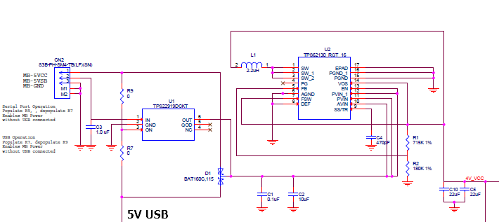
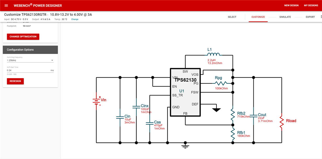
I have an implementation of the TI reference design for a 5V input to step down to 4V with the TPS62130. TI support says it matches the reference design and the layout follows (duplicates) the suggested layout. However, the design does not work. It did work the first time it was powered up with board 1 so the modem module was added (which is the load) and the board did not have power. A second board without the modem was tested and the power conversion circuit did not work upon the first or subsequence power cycles. Both boards display the same characteristics. FB voltage i 0.5-0.6V, Vout is .25-.27V. The input voltage is 4.73. There is a voltage on the SS/TR pin.
At the suggestion of TI Support, I changed to a higher input voltage. I applied 15V input and the Vout increased to 0.6V but not the expected 4V. Sadly I did not bring out the PG signal as the design was space-constrained and there was no use for the PG signal. Other than debugging so lesson learnt.
Any suggestions would be appreciated.


