Other Parts Discussed in Thread: UCC27324, UCC27714EVM-551, UCC28180, UCC256404
Hi,
Hope you are doing good.
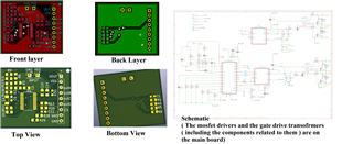
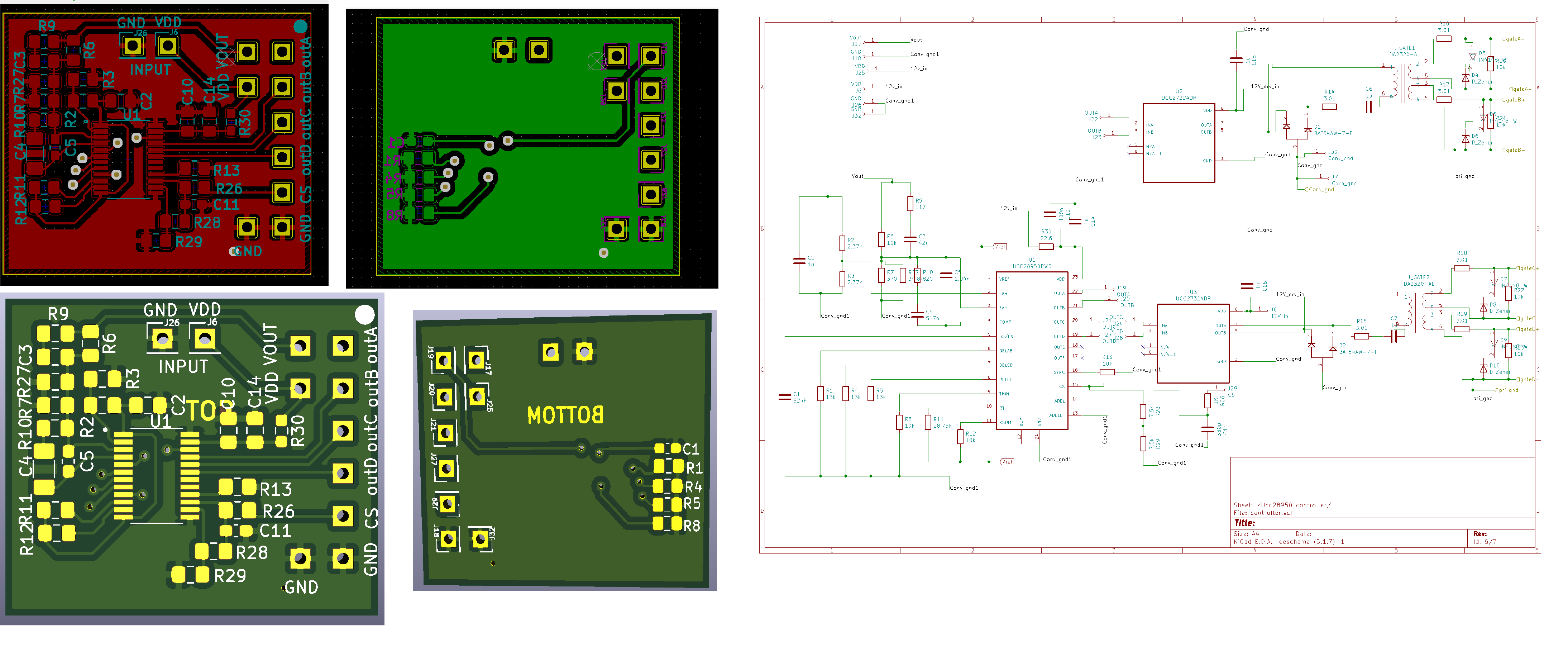
We are using ucc28950 as a controller for our 700 W design
Reference post link:e2e.ti.com/.../969039
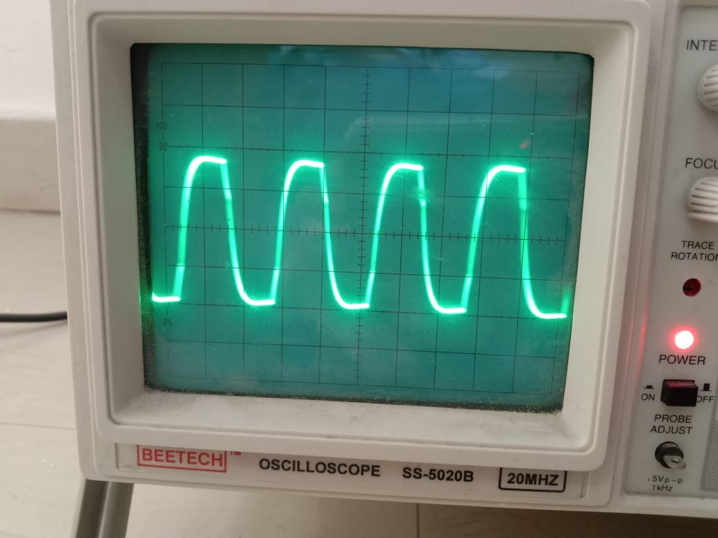
We are testing the controller alone for the gate drive signals. ( We scoped out D signal of the controller)
( Test condition : we did not power up the DC-DC board, we connected the bias supply to the controller and measured the signal)
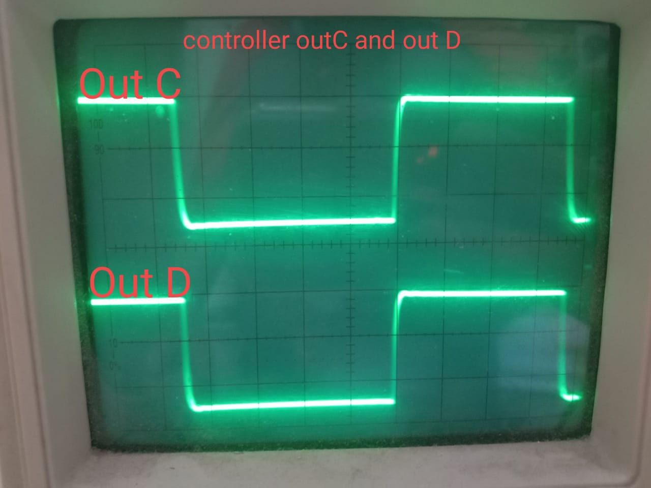
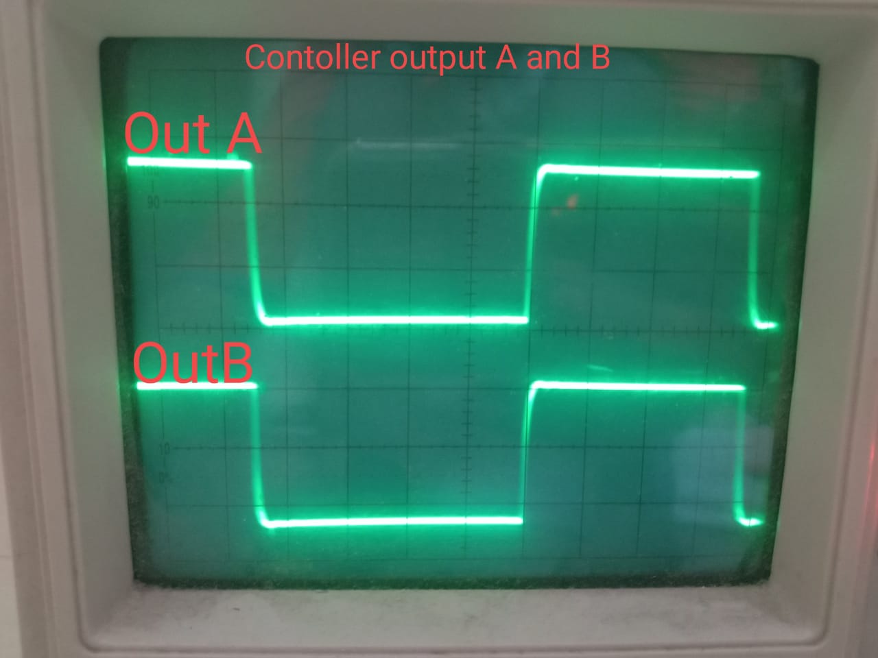
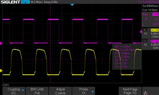
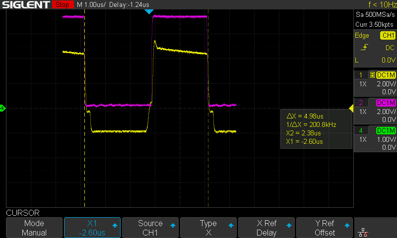
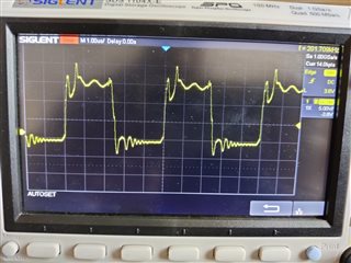
We measured the gate drive signals at the following stage :
stage 1:
output of the controller and input of the MOSFET driver IC
( division: y axis : 5V/ div, x axis : 1us/div)
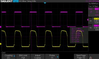
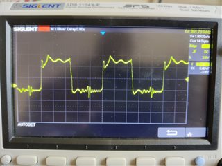
Stage 2:
The output of the gate driver IC
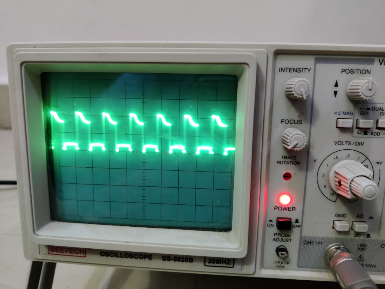
( division: y axis : 5V/ div, x axis : 1us/div)
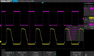
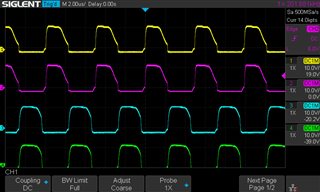
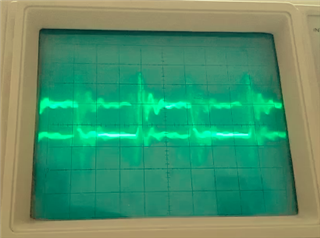
Stage 3;
Gate signal at the mosfet
initially, we observed the signal for few seconds
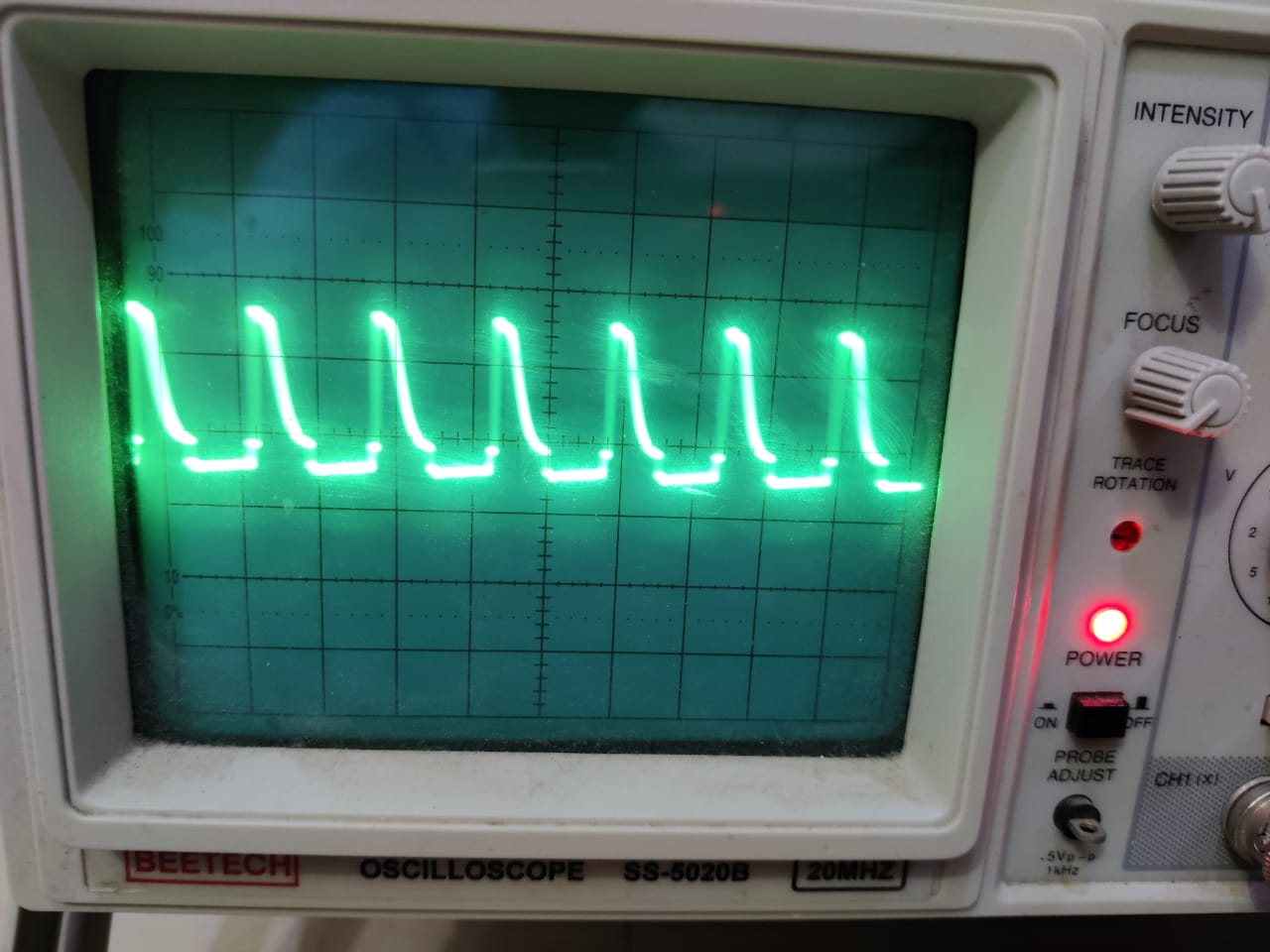
and then see that the signal is dropping down.
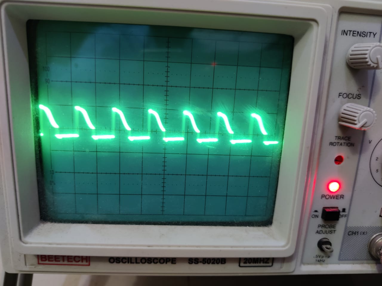
( division: y axis : 5V/ div, x axis : 1us/div)
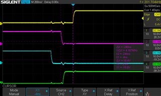
During all the processes, we observed that the MOSFET driver IC is getting very hot in the span of few seconds.
We are using ucc27324 Mosfet driver as suggested in the 600 W design application.
could you show us the waveform on how the gate signal reads at the MOSFET gate? Is our waveform expected one?
We need help solving this issue.
Thank-you
Warm Regards
Harini Krishna