This thread has been locked.

If you have a related question, please click the "Ask a related question" button in the top right corner. The newly created question will be automatically linked to this question.

BQ25570: PROBLEM DESIGN

Part Number: BQ25570

Hello,

We have created a design withe the BQ25570 charging 2 supercaps of 5F.

The photovoltaics cells are monocrystallin ref SM141K06LV.

Parameters are:

VBAT_OV = 5V

VBAT_OK = 2,2V

VBAT_OK_HYST = 2,8V

VOUT = 2V

We have 2 problems:

- when we connect cells first time teh BQ never starts and there is only 0,1V on the cells with a good sun. Cells semmes to be shorted. (Open circuit voltage on cells is about 3V)

=> To start we must put a voltage on VIN, the BQ becomes hot during a few second and after the boost reg starts normally. Volatge on cells at this time is about 2,5V)

The voltage on VBAT  reach about 3,3V

- The second problem is that the VBAT_OK never goes high so the buck reg never start.

Please could you help us to make this design working well ?

Thank you by Avance

If you want we can send you our schematic.

Regards

Thierry

  • Hi Thierry,

    If VSTOR < 2.0V when you apply power, the charger runs in cold start with is a very inefficient charge pump.  It is intended only to charge the VSTOR cap to 2.0V.  Then the main boost converter turns on.  If there is a load on VSTOR (other than the buck converter which is disabled), please remove it until the charger is up and running.

    If the voltage are putting on VIN is >= VBAT_OV, the charger turns on a pull down at VIN because it doesn't want to overvoltage the storage element (there is a path through diode from VIN to VSTOR=VBAT).  That may be the cause of the hot.

    Please attach schematic and I will review.

    Regards,

    Jeff

  • Hi Jeff,

    There is no charge on VSTOR

    The voltage on VIN is never >= VBAT_OV because it comes from a cell that has a maximum voltage of 3,3V.

    What about the buck regulator that doesn't start ?

    Please can you look at my design schematic.

    Thanks in advance for your help

    Sensor_Board_sch-V0.pdf

  • Hi Thierry,

    While I don't think it is your issue, we never tested VBAT_OK with 4.7uF on it.  Also, the schematic mentions USB power but the charger will not be boosting with 5V USB.  The pull down FET on VIN_DC will likely come on.  What is the leakage current of the zener clamp on VIN_DC?

    I don't see any other obvious errors with the schematic. 

    In cold start, the charge pump trying to raise VSTOR to 2.0V also sees the two 5F super caps through the board diode of the PFET between VBAT and VSTOR.  What is the leakage of those super caps?  The zener leakage plus the loaded charge pump might be too much for your solar panels. 

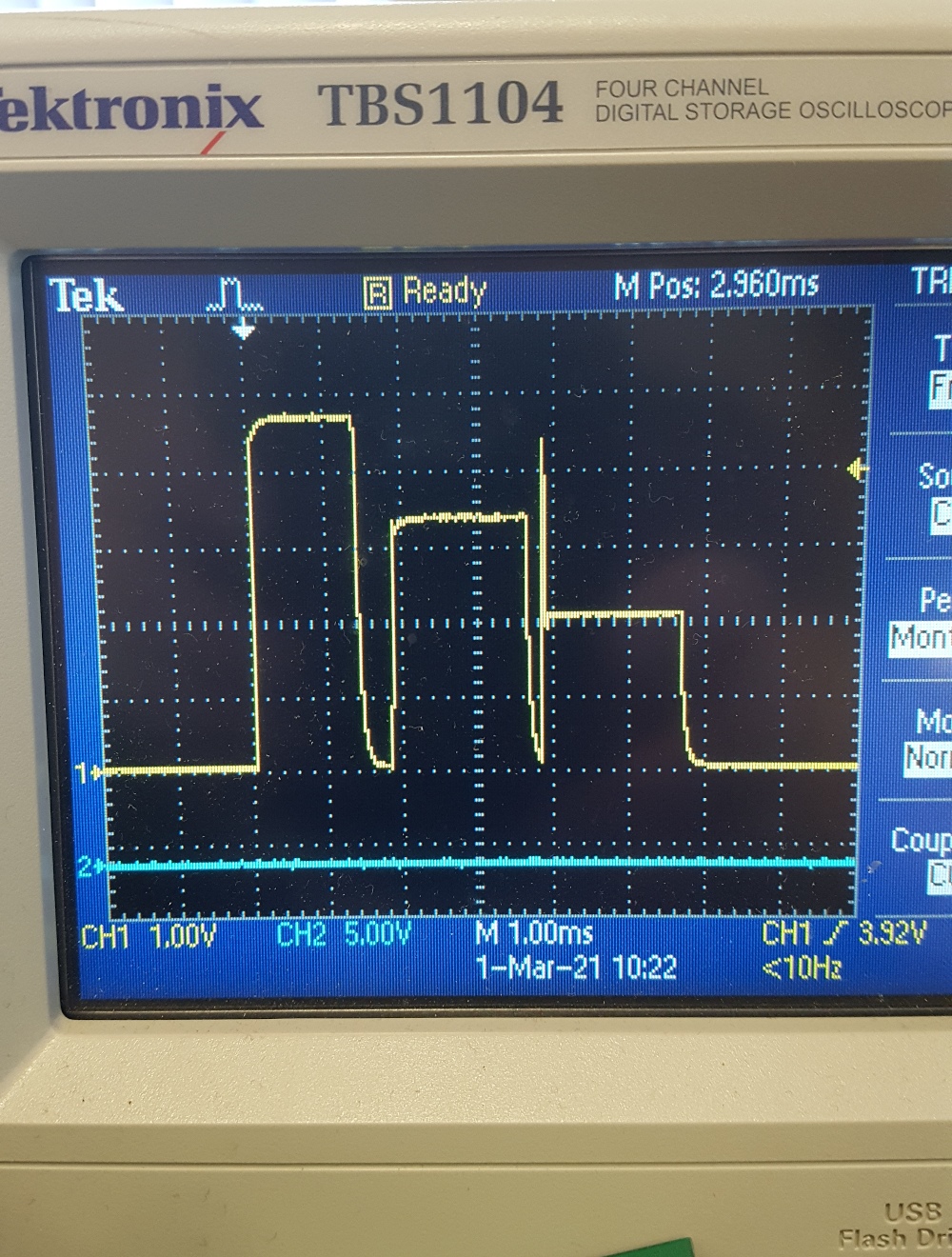
    After VSTOR>2.0V, if you take an oscilloscope plot of VRDIV similar to figure 28 on page 26, the first pulse should be VSTOR, the second 2/3 of VBAT_OV and the third (not shown in the datasheet plot) is VOUT.  Are those values correct?  If not, then parasitic solder flux resistors may be changing the threshold values as explained in datasheet section 10 page 34.

    Since your solar panel MPP is greater than 2.0V, you might consider adding a bypass FET that connects the panels directly to VSTOR, bypassing cold start.  Then when VSTOR is up, you can use a pull down FET on VOUT_EN to turn on the charger.  

    Regards,

    Jeff

  • Hi Jeff,

    Thanks again for your help.

    I remove the 4,7µF on VBAT_OK but the pin Stays at 0V. So VOUT is 0V.

    OK for the 5  USB I understand. I just put it to permit to start due to the cold start but if I can resolve the cold start I will remove the 5V USB.

    The zener is only present to protect the input of the charger if I use panel with voltage over 5V.

    You can see on the oscillogram of VRDIV that all pulses are correct. What do you thing of the spike present at the start of the third pulse ?

    So you tell me to add a PFET between VIN_DC and VSTOR, and add a NFET on VOUT_EN.  Could you send me a schematic please ?

    I don't know where I must put the gate of the PFET and how to put the NFET on VOUT_EN. I think I must monitor VSTORE ???

    Regards

    Thierry

  • Hi Thierry,

    Based on your plot, VSTOR is rising to 4.7V but is set to 5.1V [3.4V/(2/3)] but your VBAT_OK_HYST voltage is 4.8V, correct?  If so, then VBAT_OK will not go high.

    To clarify, even if you use a bench power supply instead of solar panel at VIN_DC, VSTOR does not rise to your desired output voltage?    

    Regards,

    Jeff

  • Hi Jeff,

    No in my first post I gave you parameters.

    VBAT_OK_HYST is equal to 2,8V.

    I will try tomorrow with a bench power supply but now the VSTOR is OK at 4,7V and VBAT also.

    The problem is just at start but as I put a 5V charger at first it is OK. I will design the new schematic with FET for cold start and I will send you.

    The big second problem is that the VBAT_OK pin never goes HIGH so VOUT_EN never become ENABLE.

    When I short VOUT_EN with VSTOR, then VSTOR decrease to 1V. Do you think the component is broken ?

    I will try with a other board (I have five)

    Regards

    Thierry

  • Hi Theirry,

    If you short VOUT_EN tied to VBAT_OK to VSTOR, VBAT_OK is pulling down VSTOR to ground. 

    Based on the schematic you set, the OK resistors set VBAT_OK_HYST to 4.8V and VBAT_OK =2.5V.  Please double check your resistors.  I used to design spreadsheet at .

    Regards,

    Jeff

  • Hi Jeff,

    In my schematic VOUT_EN is not tied directly to VBAT_OK, there is a 1,24MOhms resistor between.

    Sorry for the values of resistors there weren't up to date.

    In my new schematic values are updated.

    Do you think the charger could be broken ?

    I receive the evaluation board of the BQ25570. I will add the modification with FETs on it and will try it.

    Best regards

    ThierrySensor_Board_sch-V1.pdf

  • Hi Thierry,

    It is possible that the IC is damaged.  With your board not powered, can you remove the 1.24mOHm resistor and measure the resistor from VOUT_EN to GND and then also from VBAT_OK to ground?  To test whether the parasitic resistance from solder flux is an issue, can you replace the VBAT_OK resistor with 10X lower values?

    Regarding the 1.24MOhm resistor between VBAT_OK and VOUT_EN, VOUT_EN is not typical logic high and needs VSTOR-0.4V to be high.  If there is any leakage into VOUT_EN pin, the voltage drop from VBAT_OK to VOUT_EN could be higher than 0.4V.  

    Regards,

    Jeff

  • Hi Jeff,

    Thanks I will do these tests on friday because tomorrow and thursday i will be out of office.

    I am very surprised that VBAT_OK never goes high.

    Regards

    Thierry