This thread has been locked.

If you have a related question, please click the "Ask a related question" button in the top right corner. The newly created question will be automatically linked to this question.

TPS2120: TPS2120 (YFP) Package 20-Pin WCSP

Part Number: TPS2120
Other Parts Discussed in Thread: TPS2121

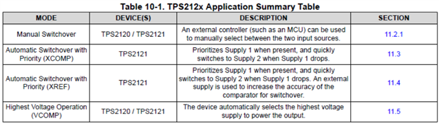
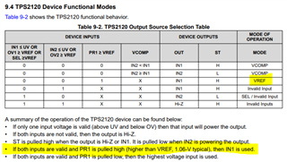
We are using TPS2120 power Mux with (YFP) Package 20-Pin WCSP in the circuit boards, currently our circuits are designed to work in "Highest Voltage Operation (VCOMP)" as in the datasheet, connecting pins PR1 & SEL to Ground. limiting the ILM to 1.5A.

Among the fabricated & assembled 7 no's of boards only 3 no's of boards are working perfectly as per the datasheet when both inputs are varied & tested. other 4 no's of non working boards have major issues while tested. in one board status ST showing high, even when both inputs are ON with same voltage of 12V. in other 2 no's of boards input 1 is not working, only when source is given at input 2, output is working as per the input. but when source is given from input1 disconnecting input 2, output is zero. in the 4th board both inputs are not working when we source the supply from inputs 1 & 2, output is Zero.

Input voltage at what we are sourcing & testing the device is at 12V.

kindly let us know what may be the issue? is that may be of manufacture or assembling issue in the IC. as its BGA kind of IC, its difficult to check the behavior at particular pins. also we have considered the layout guidelines as per in the datasheet.

kindly suggest us to resolve this issue or let me know the alternate way to solve the problem at earliest.

  • Hi Harsha,

    Please provide your schematic for us to take a look over. Also we would like to see waveforms that describe the event. Please probe, VIN1, VIN2, VOUT, ST and IOUT if possible. If the device is comparing voltages, is there any priority set? If not, you could run into the situation where the device gets stuck bouncing between the two inputs as the sources are loaded and unloaded.

  • Hello Shreyas, 

    Thanks for your response.

    PR1 & SEL pins are grounded. I can share the waveforms on 8th March, as you mentioned. please find attached the schematic of the TPS2120. Output of this TPS2120 is given to the LDO input of TPS7B6750Q with input electrolytic cap placed with value 47uF,50V,20%,SMD. 

  • Hi Harsha,

    Is it possible for you to retest this but to add some sort of priority in place? My suggestion is to set the system to prioritize IN1 at 11V and above. I am wondering if the situation that I described in my last post is causing some of the devices to bounce between the inputs as they get loaded an unloaded since they are the exact same voltage.

    I also noticed that your SS cap is only 10nF and your ILIM is set to under 1.5A  but you have a large output capacitance of 200uF. Please make sure that the inrush current caused by these output capacitors is not causing the device to hit its current limit. An easy test for this is to switch out the SS cap for a larger value, lets say 100nF or even 1uF.

  • Hello Shreyas,

    As per your suggestion i have changed the SS cap to 1uF in one board & set the IN1 to 11V & IN2 to 12V but still the ST line is fallowing the IN1 showing high. Also even when IN1 & IN2 are equal i.e. at 12V ST is showing high fallowing the IN1. only when IN1 is removed it shows low. 

  • Hi Harsha,

    Please set a priority in the system using the PR1 pin. How have you set up the priority here? Also please share scopshots that describe this event. 

  • Hello Shreyas,

    As per mentioned in the first post, we are using in the mode "Highest Voltage Operation (VCOMP)"  where the device automatically selects the highest voltage supply to power the output as per the datasheet under the section Figure 10-15, as per this PR1 & SEL to be set ground. the same is been implemented in our circuit. also as in the Table 9-2. TPS2120 Output Source Selection Table below, when both IN1 & IN2 is with equal voltage then OUT should be IN2 with ST pin low, this is not happening as in table

    I have also shared the schematic in the second post for your reference, where we have grounded PR1 & SEL to ground. kindly check & suggest some solution.

    And in other 2 no's of boards as i have mentioned in first post, even when IN1 & IN2 is sourced with the supply voltage only IN2 supply is working, IN1 is not working w.r.t output. when IN2 is removed/disconnected. 

  • Hi Harsha,

    Highest voltage mode of operation will always prioritize the highest voltage. When you are running a system with similar voltages, you could run into a situation where the device keeps switching between the two inputs as the drop and rise when being loaded and unloaded. When this happens, the device output would not be able to rise high and the device may get stuck in an error state. This is the benefit of setting priority and thereby forcing the device to stick with one input until it has dropped sufficiently enough (up to your system requirements) before switching to the second input.

    For the boards where IN1 is not working altogether, I would like to see a voltage waveform of this. There is no certainty that what is happening on one board is the same thing happening on another. For this board, I would like to see IN1 rising, ST, VOUT and IOUT if possible. There is a possibility that the device is either damaged or incorrectly populated. Another cause could be that you might be triggering the current limit due to the larger output caps. What is the total load? ST is high Z (pulled high externally) whenever IN1 is selected or when a fault is triggered. 

  • Hello Shreyas,

    As per in the datasheet of TPS2120, it has mentioned that when both input has equal voltage OUT will be IN2 & ST will be low. as in below image. i have also checked by reducing the IN1 voltage & increasing the IN2 voltage & vice versa still the ST line is high fallowing the IN1. moreover this is also working fine in other 3 no's of boards when both inputs are at 12V. as i have informed in first post, only other 4 no's of boards have issue.

    Also TPS2120 does not have Automatic switchover with Priority as in TPS2121. hence PR1 & SEL is Grounded. find attached the image as in datasheet application.

    wondering how it worked in 3 boards without any issue & how in one board ST pin shows High even when both inputs are equal & when only IN1 is removed OUT is fallowing IN2 or else OUT fallows IN1 only.


    For other 2 boards where IN1 is not working kindly find the waveform image attached as per your suggestion, i have measured IN1, OUT & ST lines. Channel 1 is IN1, channel 2 is OUT & channel 3 is ST lines. when IN1 is applied with the source voltage from 2.7V to 4.4V of the supply. OUT is fallowing the IN1 when IN1 is increased >4.4V OUT is OFF(goes Zero) as in the waveform. i have also increased the voltage till 12V & ST is working as per the voltage divider when IN1 is increased, but the OUT is OFF after 4.4V till >12V. load current is less than 70mA. 

    As per the last post, i have sent the board to check the component placement is properly or not. if not told to reassemble the component.

    kindly check & let me know your feedback.

    it will be better to have a short call with you to communicate & share regarding the issues. so if possible, kindly share me your teams mail id to have a short discussion on this issue.

  • Hi Harsha,

    TPS2120 does have priority with auto switchover. It is called VREF mode. In Table 9-2, it is the third row.

    You can use a resistor divider on VIN1 to set this. The device will run in VREF mode till PR1 falls below 1.06V and then will go back to working in VCOMP mode. For voltages of the same level, this is a better mode of operation because loading and unloading power rails will naturally cause them to fluctuate in voltage which may cause unwanted switching. device to device variation could explain why in some boards, you are seeing it work and in others, the device might be switching constantly. This is an easy fix to eliminate one potential source of error since your schematic has provision for a PR1 resistor divider network.

    In your attached scopeshot, it is a bit difficult to read as there are no measurements. Have you confirmed that the OV resistors are set up correctly and that the device is not hitting current limit? Do you have a current probe with which you can test this. Does the device try to restart after 25ms? As mentioned previously, ST will be floating (pulled high in this case) whenever IN1 is selected or a fault is taking place.

  • Hello Shreyas,

    Thank you for your update, I will make the priority PR1 pin as voltage divider & set the voltage & will see the behavior of ST pin. actually as per our application circuit need to continuously operate in IN2 only, when IN2 goes low or removed it has to consider from IN1. no issue we can increase the PR1 voltage divider top resistor to set to more than 12V so that IN2 will be considered as OUT till 12V. will check & update on 15th march.

    For the other 2 boards on IN1 not working - OV resistors are set up correctly & the device is also not hitting the current limit, because it was tested & the same value has been used for all other boards which are working fine. actually current probe was not available while testing, so measured in the multimeter by keeping in current mode. as i observed there was no restart happening even after 25ms. anyhow i have sent this board to check the TPS2120 component placement was properly mounted or not, once i get the feedback will test it  again & update you. 

  • Hi Harsha,

    If you set the PR1 to above 12V on VIN1, you will see no change of behavior from what it is now. The device will default to VCOMP mode and it will just function as it has been. If VIN2 is your primary supply, I would highly recommend flipping the inputs and setting a priority under 12V on that main rail (currently VIN2).  This will help prioritize your main supply until for example 11V, after which the device will flip to your back up rail (currently VIN1).

    In fact flipping the inputs is a good way of testing if there is an issue in populating the device since if you are able to pass the VIN2 rail through the VIN1 channel, then there is something else going on on the input side of the powerMUX. I still think we need a current probe measurement on the rail because a multimeter may not have the definition to spot the high current pull. Let me know what you find on the 15th.

  • Hello Shreyas, 

    As suggested by you, I have flipped the inputs & set the voltage divider at PR1 to 11.6V. when supply is given to both IN1 & IN2 for 12V with 2 different power supply, ST is showing high. when IN1 is reduced to <11.5V keeping IN2 at 12V, ST is still showing high. as voltage decrease or increase, ST value also decrease & increase at IN1. it is fallowing the IN1. it is not switching to IN2 even when IN1 is at lesser volts. as in evaluation board PR1 voltage dividers are set but couldn't see any changes. sorry current probe is not available to test the current. kindly recheck & suggest some solutions. 

    For IN1 not working boards will check & update you on 17th, once after i received the boards. 

  • Hi Harsha,

    For the boards you just tested, could you please provide a detailed scopeshot that shows IN1, IN2, VOUT and PR1?  Due to the variety of issues seen, could you also let me know what the previous behavior of the boards? By my understanding, it was the same as before which means that these boards could also be incorrectly populated but the issue is affecting IN2 (as compared to the other boards that show IN1 issues) or that IN2 is damaged. 

    What happens on this board when only IN2 is provided to the device?

  • Hello Shreyas,

    As suggested, kindly find the scope shot of the issue. where channel 1 - IN2, channel 2 - IN1, channel 3 - ST, channel 4 - PR1 of the attached oscilloscope image. IN1 & IN2 is sourced with 2 different supply with 12V, where as IN1 is varied to check the switch over by keeping IN2 to 12V.

    when IN1 is removed & only IN2 is connected from the supply 12V, varied the IN2 voltage by increasing & decreasing but board is working fine only issue found was ST status not changing. ST is fallowing the input IN1 when voltage is increased or decreased. as in the scope image.

    I can also send this board to recheck on component population, kindly check & let us know.

  • Hi Harsha,

    What is the event that is happening here? Is this waveform replicated on VOUT? ST following the IN1 voltage is acceptable/expected since it is connected to IN1 via a resistor divider network. Secondly, because the voltage recovers, there might be a situation where the device does not switch to IN2 because IN1 has gone high again. When testing, please drop the voltage of IN1 and keep it there. ST does not cause a switch but only exists to signify when the channel switches.

    Does the device ever complete a switchover from IN1 to IN2 or vice versa? 

    Could you please test this on an EVM and see the result? You can get an EVM for free at http://samples.ti.com. The EVM is 

    TPS2120EVM-042.

  • Hello Shreyas,

    As per in the previous post scope shot shared,  the waveforms are captured at the input side for IN1 & IN2, but not at the VOUT. as the scope which i measured is only having 4 channel so i could only measure IN1,IN2, ST & PR1. but the observation at VOUT voltage is same as IN1. as As per in the waveform i have just varied the IN1 voltage from 12V to less then 8V & increased from 8V to 13V. but i could not see the ST status change even when IN1 is at 8V as per datasheet when IN1 is at lower volts it VOUT has to switch to IN2 which is having 12V & ST pin should change the status. 

    ST pin is only changing the status only when IN1 is less then 2.7V or when IN1 supply is removed. during these 2 sceneries only VOUT switches the supply to IN2. otherwise VOUT & ST both will be fallowing the IN1 only.

    I will try to get the EVM board & will test. but can you also please confirm on the below assembling points as we currently fallowing the wafer chip package handling guidelines for assembling which is available in the TI web links attached below for your reference. 

    kindly request you to suggest package handling, assembling & protection guidelines for this type of package as it's too small package for handling i.e only 1.5mm by 2mm BGA. also please suggest if any bigger package or alternate part for the same IC

    WCSP package HANDLING GUIDE

    https://www.ti.com/support-quality/faqs/wafer-level-chip-scale-package-faqs.html

    https://www.ti.com/lit/ml/sszqnf6/sszqnf6.pdf?ts=1614853820082&ref_url=https%253A%252F%252Fwww.ti.com%252Fsupport-quality%252Ffaqs%252Fwafer-level-chip-scale-package-faqs.html

  • Hi Harsha,

    Those documents are the correct ones to follow for package handling.

    TPS2121 is a slightly bigger device and is capable of handling higher currents. It is not WCSP but can perform the same switching behavior as TPS2120 can except for manual selection. Would this device be acceptable? Please let me know how the testing on the EVM goes.

  • Hello Shreyas,

    we tried ordering for EVM free samples with the links which you have shared, but we are not authorized to get free samples. is there any alternate way of ordering.

    Thanks for suggesting TPS2121, we have ordered 2 no's of component for testing. once after the testing is done, will update on the TPS2121 results. 

    I have attached the TPS2120 boards assembly process,  PCB layout (of 4 layers) & assembled component X-ray report. kindly review & let me know your comments & feedback if there are any changes w.r.t document which we are fallowing.

    Assembly_process_PCB_&_Xray_report.pdf

  • Closing this thread out and following up through direct email.