This thread has been locked.

If you have a related question, please click the "Ask a related question" button in the top right corner. The newly created question will be automatically linked to this question.

ISO5852S: Gate driver problem.

Part Number: ISO5852S

i , I'm jaehoon kim Ph.D studeont in Seoultech university.

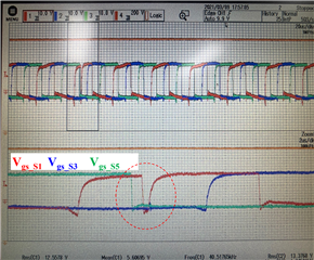
I use ISO5852S for the 3-phase converter. But when the gate signal should be on, it suddenly turns off and then turns on.

Please advise.

* Condition

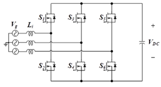
- Topology : 3-phase converter

- Turn-on voltage : 15V

- Turn-off voltage : -5V

- Desat Fault function : don't use (Desat pin was connected to the GND)

- Situration

: All switche's Duty is 0.5 and each legs have a 120 degree phase shift.

when switch S6 is turn-on, the Gate signal of S1 is drop to the Negative voltage and re-turn on.

Please let me know how can i solve this problem.

Thank you
  • Jaehoon, 

    Are you seeing FLT/ RDY triggered at this time. is VDD dipping and causing UVLO? Can you share a detailed schematic along with the signals i mentioned at the time of the false-turnoff?

    Please, an actual scpoe capture, rather than a photograph of the scope screen is much easier to read. 

    Best

    Dimitri

  • Thank you for your reply.

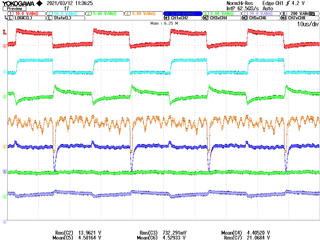
    I have attached the waveform which you requested.

    I didn't use Desat function, so Desat pin is connected to GND2.

    Please advise.

    If you can't see it well because the photo is blurry, please provide your email address.
    I will send it to you by e-mail.

    Thank you.

  • Jaehoon,

    Thank you very much for sharing these details. This is helpful.

    FLT is not tripping.  if it were, output to VGS would be cut and would go into STO, you would need to RST to get it to start again. (thought it seems there is a false turnoff on VGS about midway in the scope capture.

    To me this seems like there is a LOT of interference which is coupling to the primary side / FLT, as the dips on FLT correspond with DIPS on RDY. FLT should not be this noisy.

    Desat pin is moving a lot with respect to GND2 nearly 2V up and down, is it really tied to GND2? I think what we need to do is find the source of the interference, this is very significant on FLT2.

    I have following questions:

    1) Can you share the rest of the schematic including IGBT?

    2) Can you share layout of the driver?

    2) Can you check soldering on FLT pin and confirm the connection of DESAT pin?

    3) Is this affecting ALL driver boards which you have, or just one driver board?

    4) What is the load you are driving? Is there any possible source of interference to primary side you can think of?

    After this i have some debug steps i think we should perform first:

    1) Place 100pF caps from FLT to GND1 AND from RDY to GND1 -> Does this solve?

    2) Disconnect the comparator U3 from FLT, and resolder the pullup resistor. Does this solve?

    3) If you have a known working driver board, swap ISO5852S between the known good board and this board which is having FLT issue. Does this solve?

    4) If you do not have known working driver board/only have one board, swap the IC on the board with a fresh ISO5852S. Does the issue persist?

    Best

    Dimitri

  • The circuit is 3
    FLT is not tripping. if it were, output to VGS would be cut and would go into STO, you would need to RST to get it to start again. (thought it seems there is a false turnoff on VGS about midway in the scope capture.
    --> yes i agree. if FLT is tripping, then i need to RST to start again.

    To me this seems like there is a LOT of interference which is coupling to the primary side / FLT, as the dips on FLT correspond with DIPS on RDY. FLT should not be this noisy.
    --> As i know FLT and RDY is output signal. I think DESAT, VCC1 and VCC2 voltage are not fault condition. Even so, If FLT is get noise, then VGS can be cut?

    Desat pin is moving a lot with respect to GND2 nearly 2V up and down, is it really tied to GND2? I think what we need to do is find the source of the interference, this is very significant on FLT2.
    --> yes DESAT pin is connected to the GND2. i attatced schematic of all circuit.

    I have following questions:

    1) Can you share the rest of the schematic including IGBT?
    --> I attatced file.

    60kw_dcdc_converter_src_sec_ver.pdf

    2) Can you share layout of the driver?
    --> I attatced file.

    PHENIXON_60KW_DCDC_CONVERTER_SRC_SEC_GATE_200701-FINAL.pcb

    2) Can you check soldering on FLT pin and confirm the connection of DESAT pin?
    --> yes. i already confirm the connection.

    3) Is this affecting ALL driver boards which you have, or just one driver board?
    --> all driver board(all FET) have this problem.

    4) What is the load you are driving? Is there any possible source of interference to primary side you can think of?
    --> I attatched real converter circuit. And Vin=750Vdc, Vo=1340Vdc, Po= 0W
    And If i use a DC power supply(made by REGATRON company) as the input source of the converter, there is no problem with the gate being turned off. The waveform at this condition is attached. However, this problem occurs when the inverter developed by us is used as an input source. therefore i think noise is generated from the Input source of the converter.

    After this i have some debug steps i think we should perform first:

    1) Place 100pF caps from FLT to GND1 AND from RDY to GND1 -> Does this solve?

    2) Disconnect the comparator U3 from FLT, and resolder the pullup resistor. Does this solve?

    3) If you have a known working driver board, swap ISO5852S between the known good board and this board which is having FLT issue. Does this solve?

    4) If you do not have known working driver board/only have one board, swap the IC on the board with a fresh ISO5852S. Does the issue persist?

    I will do this debug steps, and i will share resurlt.

    thank you.

  • Jaehoon,

    Thank you for the details.

    4) What is the load you are driving? Is there any possible source of interference to primary side you can think of?
    --> I attatched real converter circuit. And Vin=750Vdc, Vo=1340Vdc, Po= 0W
    And If i use a DC power supply(made by REGATRON company) as the input source of the converter, there is no problem with the gate being turned off. The waveform at this condition is attached. However, this problem occurs when the inverter developed by us is used as an input source. therefore i think noise is generated from the Input source of the converter.

    Yes this is a real possibility that this noise can be coupled  to primary side, which adding filter capacitance will help. Please let me know the updates of your debug steps which i proposed and any further debug steps you are taking. The large di/dt of the inverter and magnetics can cause issues. One extra step is you could try blocking the interference from your inverter supply with a large piece of metal to block the EMI, but it sounds like we already know that it is already a cause of the issue.

    Secondly, cannot import your PCB design using PCAD, tango, or Mentor. If you can send gerber of it it will be helpful.

    Best

    Dimitri

  • I attached gerber data file. please check the layout.
    And can you answer to my question?

    To me this seems like there is a LOT of interference which is coupling to the primary side / FLT, as the dips on FLT correspond with DIPS on RDY. FLT should not be this noisy.
    --> As i know FLT and RDY is output signal. I think DESAT, VCC1 and VCC2 voltage are not fault condition. Even so, If FLT is get noise, then VGS can be cut?

    PHENIXON_60KW_DCDC_CONVERTER_SRC_SEC_GATE_200701-거버.zip

    Thank you.

    Jaehoon kim

  • Jaehoon,

    As i know FLT and RDY is output signal. I think DESAT, VCC1 and VCC2 voltage are not fault condition. Even so, If FLT is get noise, then VGS can be cut?

    This is correct, to an extent.

    DESAT, VCC1/2 Voltage are not in fault condition according to your scope shots.

    My guess is that the one place we see VGS fall, the noise couples strongly enough to IN+ that it falls below IN+'s VIL threshold, turning the driver off, before recovering back above VIL and then VGS goes high once more.

    This is why i asked you to check IN+ as well. We should see whether IN+ is getting noisy enough to fall below VIL, this would be very bad for the system. Regardless of whether or not the secondary side is not creating faults, having this huge noise on the input poses issue like the one i just mentioned. Please let me know if you have any updates.

    I am installing PADS now to take a look at your gerbers / layout. Seems that altium doesn't like the files.

    Best

    Dimitri