This thread has been locked.

If you have a related question, please click the "Ask a related question" button in the top right corner. The newly created question will be automatically linked to this question.

CSD17573Q5B: Land pattern recommendation with vias under thermal pad?

Part Number: CSD17573Q5B


Right now in one of our designs, we are using the CSD17573Q5B, but this question should apply to all Q5B devices (and I would say Q5A devices using the Q5B footprint since another thread indicated that Q5B footprints can be used for Q5A devices: https://e2e.ti.com/support/power-management/f/power-management-forum/602226/csd19534q5a-footprint-mismatch-on-recommended-pcb-pattern-son-5x6)

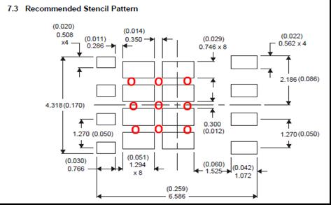
The recommended PCB pattern and stencil pattern on page 9 of the datasheet (https://www.ti.com/lit/ds/symlink/csd17573q5b.pdf) does not include thermal vias.  To improve heat dissipation in our PCB, I would like to add vias underneath the thermal pad to connect to copper pours in the other layers.  My main concern in doing so is this would affect the stencil openings since the vias would wick away solder.

My assumptions are that the solder openings would need to be increased a little to compensate for solder going into the vias.  I am intending on using 0.30 mm tented vias.  From my research, I believe that vias should not be under the stencil openings themselves but other than that I have not been able to figure out how to go about adjusting the stencil opening size.

Can TI provide a footprint for Q5B with thermal vias?  Or otherwise guidance on modifying the current recommended stencil pattern when adding vias would be appreciated.

Thanks,

Charlie

  • Charlie,

    Firstly, thanks for using our FETs.

    I know people use thermal vias, I am looking to get the specifics from our SMT experts and will come back to you as soon as I can

  • Charlie,

    I just remembered TI has a QFN/SON application note that has via recommendations on page 7, here: https://www.ti.com/lit/an/slua271b/slua271b.pdf?ts=1615405906464&ref_url=https%253A%252F%252Fwww.ti.com%252Fpower-management%252Fmosfets%252Fsupport-training.html

    Let me know if you need anything else.

  • Charlie,

    In addition to the document above our SMT expert also suggests the following:

    1. Thermal vias size 0.2mm would reduce solder wicking due to surface tension.
    2. Try to locate the thermal vias not directly underneath the solder paste.
  • Hi Chris,

    Thanks for sharing that app note. It is a very helpful reference. I've read through section 3.4 on Exposed Pad PCB Design and 4.4 on Exposed-Pad Stencil Design. I do have a question after reading those sections. I am using the "Recommended Stencil Pattern" on page 9 of https://www.ti.com/lit/ds/symlink/csd17573q5b.pdf as a starting point for the stencil design for Q5B packages. The recommended PCB pattern on the same page does not include vias underneath the thermal pad, and I am going to be adding thermal vias.

    My questions are:


    Since I am deviating from the recommended PCB pattern by adding vias, do I also need to deviate from the recommended stencil pattern by increasing the stencil openings underneath the thermal pad?
    Are there any app notes or guidelines pertaining to calculating how much bigger the stencil openings need to be, assuming the answer to question 1 is "yes"? I am guessing this depends on stencil thickness, via drill size, whether tenting/plugged or unmasked, and board thickness.
    Regarding the suggestions from your SMT expert, well-noted, thank you. We will probably try 0.30 mm vias for cost reasons, but they will be tented and will not be placed directly underneath the solder paste.

    Charlie

  • Charlie,

    I managed to get the following inputs from our SMT experts:

    1. If the vias are tented, then 0.3mm will be good.
    2. Normally we try to put vias between the gaps to avoid
      solder wicking. (See below drawing for example).
    3. We designed the stencil aperture with consideration of
      3 major factors:
      Balancing the solder coverage,
      Thermal conductivity,
      Passage for outgassing to minimize solder voids.
      So I would suggest to follow TI recommendation.

  • Chris,

    Great, thanks for the clarification.  We will use 0.30 mm tented vias placed in between the gaps in the paste and design our stencil according to TI recommendation.

    Charlie