This thread has been locked.

If you have a related question, please click the "Ask a related question" button in the top right corner. The newly created question will be automatically linked to this question.

BQ76952: CHG FET doesn't turn on

Part Number: BQ76952
Other Parts Discussed in Thread: BQSTUDIO

Hi,

I have used the following registers

COV threshold, COV delay, CUV threshold, CUV delay, OCC threshold, OCC delay, OCD threshold, OCD delay, SCD delay, Enable ProtectionsA, Sub-command 0x009A to disable sleep mode.

I am using TS1, TS2, TS3 as thermistors, DDSG, DCHG, ALERT pins are left floated, DFETOFF, CFETOFF pulled to VSS, HDQ pin is pulled down to VSS with 1K resistor.

I am facing the following problems

1. I was unable to configure TS3 i.e., even though I write 0x07 to 0x92FF ( TS3 config register) when I read it again.. It doesn't change its value from default state i,e., 0x00 , whereas I have set TS1, and TS2 successfully. What could be the issue?

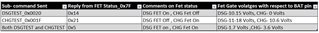
2. When I send the FET_ENABLE-0x0022 subcommand, only DSG FET is being turned on but CHG FET is not turned On

Some Information

  •   I have checked Safety Alert A, B, C and Safety Status A, B, C all were at 0x00
  • I am Testing the BMS with a 16s pack, Voltage of the pack is around 58V, DSG Fet Gate voltage with respect to Battery negative around 68V but CHG Fet gate voltage is only around 58V ( so CHG Fet is not turned ON right?)
  • Instead, FET_Enable when I replace it with CHGTEST-0x001F, DSGTEST-0x0020 sub-commands CHG gate is 61V, DSG gate is 59V

Kindly help with, what main registers should be changed from default to turn on FETs properly and discharge pack because with only DSG FET turned on when the load is connected both FETs are being turned off and Voltage between Pack + and Pack - is zero

  • Hi Mounish,

    Regarding issue #1, there should be no reason you cannot write to the TS3 configuration. Maybe you have an error in the checksum calculation? Are you using BQStudio?

    For #2, it is possible the device is in SLEEP mode and by default the CHG FET will turn off to conserve power. The SLEEP_DISABLE command will prevent the device from entering sleep, but if you write to RAM registers afterwards (by entering and exiting CONFIG_UPDATE mode), it will re-enable sleep based on the setting of the [SLEEP] bit in the Power Config register. If you want to change this CHG FET behavior, you can set the [SLEEPCHG] bit in the FET Options register to zero.

    Best regards,

    Matt

  • Hi Matt,

    Regarding the TS3 configuration issue, I am not using BQStudio. I don't think I have a checksum error because with the same function I was able to turn on REG 1 and REG2. additionally, I have changed the TS2 configuration to 0x07 from its default state of 0x00. Is it possible that the register may damage? or any special care should be taken TS3 register.

    For #2

    I have set the Power_config register as recommended, but I  see a very little boost on MOSFET gates. Let me share with you the results of my test, where I sent only the following commands.

    When both FET turn-on subcommands are sent, gate voltages are dropping down. I think the charge pump is unable to boost both of them at once. Can a defective BJT cause this problem? ( Find my schematic below). The voltage difference on the CP1 capacitor is around 10volts is this ok?

  • Hi Mounish,

    There should be no issue writing to TS3 Config. Maybe you can share the exact data sequence you are writing along with the checksum.

    On your schematic it looks like Q3 is backwards. That means the gate of the DSG FET will only be a diode above the source when the DSG pin is high. The voltage on the CP1 cap sounds okay - it is typically around 11V.

    For the FET commands, you can also use ALL_FETS_ON(), ALL_FETS_OFF(), CHG_PCHG_OFF(), and DSG_PDSG_OFF() - this way you can use these in normal operation and do not need to use the FET Test mode.

    Matt

  • Hi Matt,

    Thank you so much, After eliminating q3 from the circuit gate voltages are perfect. Just one final question.

    • I am using a 2.5mOhm sense resistor, so I have set CC gain to (7.4768/2.5) = 2.9907 as recommended in the calibration and OTP programming guide.
    • All protection registers CUV, COV, OCD1, OCD2, SCD  Autonomous cell balancing, Autonomous Fet control bits were set.
    • I have Enabled Protections A, No safety fault is triggered

    When I try to draw 5A amps..everything was normal but when I increase the load BMS is tripping off, Even If I increase OCD1, OCD2 protection thresholds to the max, BMS is tripping. What could be the problem? (Problem1)

    My test results:

    when I monitor results CC2- 0x3A

    When no current is drawn - 65533

    When around 5Amps ( I am using an analogue ammeter) is drawn - 32769

    When more load is added - Trip

    (Problem 2 ) Please explain how CC2 should be scaled to show the correct current ( I have not changed the DA configuration register )

  • Hi Mounish,

    Are you writing the CC Gain register using 32-bit IEEE-754 floating point format? It seems you are getting some very strange readings for the current measurement.

    Matt