This thread has been locked.

If you have a related question, please click the "Ask a related question" button in the top right corner. The newly created question will be automatically linked to this question.

LM5066: GATE pin is not working after the output is shorted and come back to normal

Part Number: LM5066

Hello TI experts,

my customer is now designing LM5066 for their power supply, and made 1st PCB, there is problem.

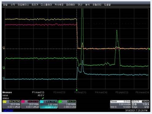
overcurrent protection works well. if they put overcurrent condition, the power delivery stops, and back to normal current, the power delivery start again.

but in short protection, it does not come back to normal.

we short CN5 pin, the power delivery stops. but after release the short in CN5, power delivery does not start again. (actually we cannot see the output from GATE(pin2) pin.)

here is the schematic below. can you check it for our problem?

(CL(pin22) is connected to VDD, to set the overcurrent threshold to be 26 mV)

test condition is as below;

  - input voltage : +52Vdc ~ +53Vdc

  - output current load : 0A ~ 1.8A

please check this issue. Thanks.

Best regards,

Chase

  • Hi Chase,

    Can you share below details to debug

    1. Test waveform of Vout, Timer, GATE and input current during short circuit test.

    2. Filled up design calculator

    3. What is the startup load at the output ?

    Best Regards, Rakesh

  • Hi Rakesh,

    Here is more information you asked;

    1. during short circuit test, Vout, Timer, GATE are 0V, and initial input current is 1.6V

    2. here is design calculator;

    LM5066 Design_Calculator_REV_B_0317.xlsx

    3. startup load current is 1.6A

    and here is some values of parts

    Rsns = 12Mohm

    Rpwr = 150Kohm (calculated value was 30Kohm based on datasheet, but it did not work so they found another value)

    Ctimer : 150nF

    MOSFET : FQD13N10LTM (Fairchild)

    as i said, overcurrent protection works well(insert 52V/2.2A->output stopped) and it come back to normal when overcurrent is over.(2.2A to 1.8A)

    and customer wants the input voltage 50~53V, input current 0A~1.8A. also they want short circuit protection and overcurrent protection.

    Please check this issue. Thanks.

    Best regards,

    Chase

  • Hi Chase,

    Is customer using dvdt circuit at the GATE as shown in the schematic ? If yes - set F72 cell in the design calculator to 'YES'

    Test waveform of Vout, Timer, GATE and input current during short circuit test is missing, please get it.

    Best Regards, Rakesh

  • Hi Rakesh,

    Thank you for your reply.

    during short circuit test, these 3 waveforms are just 0V. is waveform picture necessary in this situation?

    and here is my modified design calculator, changed F72 to 'YES'.

    LM5066 Design_Calculator_REV_B_0317-2.xlsx

    if there anything wrong, please let me know.

    Best regards,

    Chase

  • Hi Chase,

    Waveform is still needed to understand the timer voltage, current profile during the fault.

    Best Regards, Rakesh

  • Hi Rakesh,

    please check the waveforms below ;

    CH1 yellow : GATE

    CH2 red : Vout

    CH3 blue : Ctimer

    CH4 green : Iout

    as you know, this IC is completely dead after each short test. this test is a huge burden for my customer.

    please check this issue. Thanks.

    Best regards,

    Chase

  • Hi Chase,

    During short, L3 causes kick-back voltage which is not well captured in the above test waveform. Use TVS diode 5.0SMDJ54A at the Vin pin of IC to clamp the transient voltages e2e-uat.ti.com/.../selecting-tvs-diodes-in-hot-swap-and-oring-applications

    Use PSMN4R8-100BSE for Q15 to have better SOA margin.

    Best Regards, Rakesh

  • Hi Chase,

    Please suggest above changes to the customer and let us know if there are any follow-up questions.

    Best Regards, Rakesh

  • Hi Rakesh,

    Thank you for your reply.

    I already guided your suggestion right after your reply.

    I will tell you if there are any updates from my customer.

    Best regards,

    Chase

  • Hi Rakesh,

    It took a long time to get the parts for test.

    the result is, it is all the same even I changed FET and diode, waveform is same too.

    could you tell me other points to check?

    also I want to tell that when LM5066 is broken because of the short output circuit, PCB routing in front of SENSE pin (#3) burns out.

    I think it is related on this matter.

    please check this issue. Thanks.

    Best regards,

    Chase

  • Hi Chase,

    You mean LM5066 failed even when you used PSMN4R8-100BSE for Q15 and TVS diode 5.0SMDJ54A at the input  ?

    Please share waveforms (similar to Figure 46 and Figure 47 in www.ti.com/.../lm5066.pdf) during short output test

    Best Regards, 

    Rakesh

  • Hi Rakesh,

    Thank you for your reply.

    fortunately they solved the problem themselves. it was because of the L3 inductor.

    after removing L3, hot-short protection is working well.

    and still I have another question.

    they use pin7 as enable(shutdown control)

    they tested it many times about it, sometimes it is working even EN is not high.

    in this situation they have to toggle EN pin in GUI. then it work properly. until then it is always working even they change the status of EN pin.

    is it a problem of schematic? or the matter of I2C communication or other SW part?

    please give me some advice about this matter. Thanks.

    Best regards,

    Chase

  • Hi Chase,

    EN pin voltage has to be HIGH to turn-ON the external FET.

    Have they probed pin-7 voltage and GATE voltage to confirm ?

    Best Regards, 

    Rakesh

  • Hi Rakesh,

    Yes, PIN7 is low, and GATE pin is high.

    and I have one more question.

    If i want to use pin7 as enable, should I refer the schematic in datasheet 8.4.4? (with 3 resostors)

    actually we used 4 resistors to set UVLO and OVLO. is it okay to control the shutdown?

    Best regards,

    Chase

  • Hi Chase,

    Yes, PIN7 is low, and GATE pin is high.

    -> Is it the same case for all the boards ? When you replace with new IC and new MOSFET on the same board  - is it fine ?

    If i want to use pin7 as enable, should I refer the schematic in datasheet 8.4.4? (with 3 resostors)

    actually we used 4 resistors to set UVLO and OVLO. is it okay to control the shutdown?

    ->The control to shutdown the device with UVLO/EN = LOW is independent of single resistor ladder or two separate resistor ladders.

    Best Regards, 

    Rakesh

  • Hi Rakesh,

    Is it the same case for all the boards ?

    -> actually it depends on the time, even in the same board. sometimes it works correct, sometimes it does not work correct.

    When you replace with new IC and new MOSFET on the same board  - is it fine ?

    -> they did not try it, just I can imagine that it depends on time.

    can you tell me the points to check more for this matter?

    Best regards,

    Chase

  • Hi Chase,

    It's very difficult to comment if the behavior is not repeatable and depends on time. Can we place oscilloscope in trigger mode to capture (GATE, input current, timer voltage, EN voltage) at that instant.

    Best Regards, 

    Rakesh