Hi,
I would like to know how the device operation in skip mode or CCM.
Depends on inductor current or output voltage?
This thread has been locked.
If you have a related question, please click the "Ask a related question" button in the top right corner. The newly created question will be automatically linked to this question.
Hi
The TPS53211 uses Rdson sensing of the low side FET to detect the zero current and turns of the low side FET to improve the light load efficiency.
To skip pulses, when the Vout becomes larger because of light load, the FB voltage becomes larger which controls the output of the internal error amplifier and is used to skip pulses.
Please let us know if you have further questions.
Regards,
Gerold
Hi Dhanabalan,
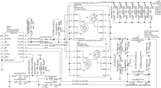
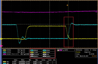
Please check the waveform and schematic.
As I know dead time is auto adaptive controlled by HS and LS Vgs voltage.
The Vgs waveform looks like shoot through, do you have any comment of the waveform and schematic?

CH1: Hi side VGS
CH2: Low side VGS
CH3: 3.3V vout


No, this does not look like shoot-through. It looks like "sub-threshold cross-over" You can see in the Channel 2 waveform that the switching node voltage begins to dip, indicating the turn-off of the low-side FET before the high-side driver beings to rise and well before the high-side gate drive reaches the MOSEFT threshold voltage.
Was the UGATE waveform taken from the UGATE pin or one of the two top-side FET gate drives?
Hi Jim,
I will close this first, please let us know if you have any further concern .
BRs,
Young
Hi Young,
I have reached to BU and discussed the issue via mail, thanks for your support and we can close the thread.