This thread has been locked.

If you have a related question, please click the "Ask a related question" button in the top right corner. The newly created question will be automatically linked to this question.

TPS54360B: Power management forum

Part Number: TPS54360B
Other Parts Discussed in Thread: TPS54360, LMR36006, LMR36015

Hi TI,

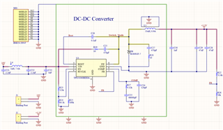
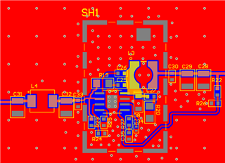
I am developing a DCDC supply for an academic project related to EMC. The design I have built on PCBs converts 24V to 3.3V and delivers 500mA. We are trying to pass CISPR 25 Class 5 emissions requirements, but every time we make changes that would traditionally work we are seeing significantly more noise and an increase in ringing. Originally we were running the supply at 680kHz, but we increased that to about 800kHz and we are seeing cleaning switching, but it is still not reacting to the EMC countermeasures the way we would expect. 

I was hoping to speak to an AE that is familiar with this IC to get their input on the design.

Thank You

Nick

  • Hi Nick,

    Please see this article series on EMI: http://www.how2power.com/other/EMI_Guide.php

    Keep points to mitigate radiated EMI include:

    (1) Use a GND plane under the power stage (with very low intralayer spacing such as 4 mils);

    (2) Use a shielded inductor with the shielded terminal (whatever end of the winding is on the inside or the bottom of the winding structure) tied to SW;

    (3) Keep the input ceramic cap close to the FETs to minimize parasitic inductance that can cause SW voltage overshoot and ringing. See app note snva803 for power stage layout best practices.

    Regards,

    Tim

  • Hi Tim,

    I was hoping to meet with an Applications Engineer to show them what I have been seeing. I am more worried that things that traditionally improve EMC issues seem to be having a negative effect on the emissions, and I want to make sure there is not an issue with how I set up the controller that is making it run abnormally.

    Thank You,

    Nick

  • Send on the schematic and layout and I'll take a look.

  • Hi Tim,

    I have include the schematic and layer one of the layout layout. Layer two is solid GND. The 24V input comes from a pair of LISNs, and a resistive load is attached to 3.3V output in order to draw 500mA. In this schematic it is set up to switch at 680kHz, but I have also tried changing the switching frequency to 800kHz. I started without the snubbers, input inductor, and shielded inductor, but have also tried all of those things and more to bring down the emissions. I just want to make sure that I have set up the basic designed properly, and that it is not running in some funky state.

    Any insight you have would be appreciated.

    Thank You, 

    Nick

  • Thanks, Nick. We also have the TPS54360 Excel quickstart calculator - that is worth checking: https://www.ti.com/product/TPS54360#design-development##design-tools-simulation

    Regards,

    Tim

  • Here are some comments on the schematic:

    If this is a 500mA design, a 3.5A converter is not really suitable (it will operate in DCM at light loads). Consider using the LMR36006 or LMR36015 instead.

    The inductor is rated for 0.9A yet this is a 3.5A converter with a 5.5A peak current limit. Check for inductor saturation.

    No need for two RC snubbers - one RC from SW to GND is adequate.

    The input filter needs damping - connect a 10uF electrolytic at the power stage input (right side of the filter inductor).

    68nF seems like a high compensation capacitance and sets up a large RC time constant on the COMP node, slowing transient response settling time.

  • In terms of the layout, the input capacitor is too far from the IC. It needs to go as close as possible to the VIN and GND pins, like where R19 is currently located. Also, the feedback resistors should be at the IC (keep the feedback trace as short as possible).

    Also, keep a solid GND plane on layer 2, with 4 mils separation to the top layer with the power stage components.

    Regards,

    Tim