This thread has been locked.

If you have a related question, please click the "Ask a related question" button in the top right corner. The newly created question will be automatically linked to this question.

TPS7A7002: TPS7A7002 Vout Error

Part Number: TPS7A7002
Other Parts Discussed in Thread: BQ24040

Dear TI,

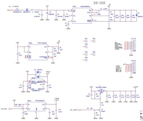
I send you the schematic of my new design.

I´ve calculated the resistor divider for an Vout of 3.8VDC in the REG2 (TPS7A7002DDA), but I always get 4.26VDC in Vout of REG2.

I´ve changed R3 by 200K (Vout=3.5VDC) and Vout is 4.26V also.

I need help please.

Regards.

  • Hello Javier,

    Can you please review the PCB for any board contaminants, such as solder flux or other residue from when the PCB was assembled?  Occasionally we have customers contact us for these types of problems, and one of the more common issues is leakage on the board.  You will want to inspect the feedback node and any leakage from Vin to Vout.

    Thanks,

    - Stephen

  • Hi Stephen,

    First of all, the input of TPS7A7002 is 4V8. I have checked the solders and everything is fine. I have assembled 10 prototypes and it happens in all of them. I have checked the PCB and seen that R3 is linked to the 3V8 plane instead of pin 6 per track. I have R3 attached per track and I still have 4.26V. I do not know what else to do...

  • Hi Javier,

    The schematic you attached is very difficult to read as it seems to have been uploaded with low resolution. Can you reattach one with better resolution? I tried zooming in and I can't make out enough to assess the schematic. It does sound like a systematic issue since it is on multiple boards and so may not involve board contaminants.

    Is this a DC 4.26V measured on a DMM or did you check with a scope? It would be good to know if the scope shows an oscillating output or not. A scope shot showing Vin, Vout, Ven, and Iout (if possible) could be very helpful with the schematic. 

  • Dear Kyle,

    I read the schematic perfectly with zoom in my computer, but I upload in pdf again.

    Yes, the measures are made with a scope.  The outputs are stables.

    I don´t know reattach documents from Reply button. How can I do? Drop in images and pdf don´t work.

  • Hey Javier,

    Thank you the schematic is now clear and I don't see any concerns with the schematic, it looks ok. It is interesting that you change R2 and you get the exact same voltage on the output. Is there current flowing from the LDO to the load?

    What did you mean by "I have checked the PCB and seen that R3 is linked to the 3V8 plane instead of pin 6 per track. I have R3 attached per track and I still have 4.26V"? Does this mean that both R3 connections are shorted to the Vout node? I'm wondering if the LDO is in dropout, Vout tracks Vin then we know it is in dropout and we just need to figure out why.

    • So if you raise Vin to 5V does the output voltage also raise by ~200mV?
    • What is the voltage measured at FB (pin 7)?
    • Can you measure the resistance of the FB node to GND and the resistance from FB node to Vout node?
      • I'm wondering if there is a short between FB and GND or if the Vout to FB node is open circuit causing this to happen on all your boards. 

    As for your question about attaching in a Reply, there is an Insert option at the bottom of the Reply and you can insert a file there. 

  • Thank you all for your responses.

    In the last assembled prototypes it works OK, perhaps it is a solder or boards contaminants.

    Best Regards.

  • Dear Kyle and Stephen,

    I just found out what the fault is and it's not flux contaminants.

    This fault occurs on the boards that have the BQ24040 battery charger mounted and I don´t understand why.


  • Hey Javier,

    Your schematics show the outputs of the TPS7A7002 and the BQ24040 are both listed as +3V8. Are the outputs of these two devices connected? If so this is the cause of the behavior that you are seeing. Looking at the BQ24040 datasheet it appears that it outputs 4.2V, so if that output is tied to the LDO's output then the voltage will be the higher 4.2V sincethe LDO does not have a pull down.

  • Dear Kyle,

    Yes, The outputs of these devices are connected. How can I solve this issue? I don´t understand where to put a pull down.

    Perhaps I chose the wrong charger chip.

    Regards.

  • Hey Javier,

    I'm not sure why you connected the outputs of two different regulators so can you explain to me what you are trying to do? If I understand what your intent is then maybe then I can provide you some ideas on how to address it. 

  • Dear Kyle,

    It is a mistake in my schematic. I want to make the equipment work with the power supply and if it turns off, let it work with battery. How to connect the battery to system load when power supply turn off? This is my question right now.

    +3V8 is the system VCC.

    Maybe this question should be in another thread. The solution to my query is answered above.

    Regards.

  • Hey Javier,

    If 3.8V is the System VCC (coming from TPS7A7002) then could you put a diode in series with the BQ24040? That would only allow the BQ24040 to provide power/current if the TPS7A7002's output was off or at least 1 diode drop below 4.2V. 

  • Hey Kyle,

    This solution is not valid, since the system voltage (between 3.6V-4.5V) when the battery works will be the battery voltage (3.7V nominal) minus 0.8V. When power supply is ON, works fine (VCC sytem is 3.8V).

    Regards.