This thread has been locked.

If you have a related question, please click the "Ask a related question" button in the top right corner. The newly created question will be automatically linked to this question.

BQ25792: OTG mode discharging issue

Part Number: BQ25792

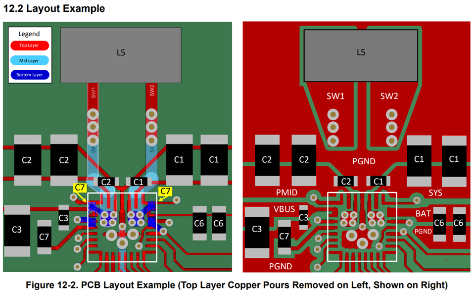
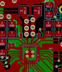
Using BQ25792 standalone IC. KICAD schematic uploaded below.  1s configuration is implemented. Boosting from 3.6V to 5V.

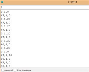
While using OTG mode the discharging current does not exceed 500mAmps. There is a LED placed at VBUS. So if the current exceeds 500mAmps the led starts blinking and current starts dropping and shuts down IC shortly.

OTG BQ25792 Schematic

KiCad Schematic


  • Hi Cyril,

    I am unable to open your files for reason.  Regarding your question, how are you measuring the discharge current?  Is there a multimeter in series between battery and the BAT pin?  If so, please remain it and try again.  A multimeter adds resistance, varying if set to autorange, and can cause issues with charging and discharging.

    Regards,

    Jeff

  • Is there a multimeter in series between battery and the BAT pin?

    Hi Jeff,

    Yes there is a multimeter in series between battery and BAT pin. I also have tried without using multimeter. Just jumping both the pins. But present issue is not about high resistance. With a proper resistance current does exceed 500mAmps but after few seconds it starts decreasing.  IOTG limit is also at 3Amps.

    Could it be IC heating issue?

    I charge at 1.5A the IC heats up but it does not shut down charging. 

    So I think it should withhold 1A of discharging easily.

  • Cyril,

    What are the status and fault registers reporting immediately after shut down?

    Regards,

    Jeff

  • Status register 1B reports  (0100 0111 )(47h) when working properly and when error occurs it reports(0000 0000) (everytime)

    Status register  1D reports(0000 0001)(01h) i.e only VBAT is present and when error occurs it sometime shows (0000 0101)(5h) (not everytime). 

    Fault register  20 reports(0000 0000)(0h) and when error occurs it reports(0010 0000)(20h) i.e overvoltage VBAT status. The incoming data is shown below.

    Register Format is as follows

    (1B,1D,20)

    This is a continuous data read from BQ25792. this goes on for 3 to 4 mins. and then 1B and 20 register goes 0 and 1D register reports only VBAT present.

  • Cyril,

    Assuming you have battery at BAT pin and you have no load on SYS, the charger is properly going into OTG mode at the beginning which means that the charger.

    But then the charger reports BAT OVP, which typically only occurs in OTG mode if there is large, fast transient load on VBUS, requiring the charger to pull high current during the transient and then goes away quickly, causing an overshoot at BAT.  Do you have such a load on VBUS?

    At the end you are in IOTG regulation, which means the OTG output current limit is being limited to the value in the IOTG regulation register (REG0x18).  What value do you have in that register?  Also what is the value in the IBAT discharge register  (REG0x14)?  That control loop could also be limiting current to OTG output at VBUS/VACx.

    Regards,
    Heff 

  • But then the charger reports BAT OVP, which typically only occurs in OTG mode if there is large, fast transient load on VBUS, requiring the charger to pull high current during the transient and then goes away quickly, causing an overshoot at BAT.  Do you have such a load on VBUS?

    Yes I do have such load on the VBUS. So basically I am controlling the current to the load using a mosfet using PWM(0 to 225). So when I set the PWM higher than 220 the current should exceed 500 mAmps. But the error occurs as mentioned in my last reply. Is there any register I am missing to set value or is there any way around it in the BMS?

    What value do you have in that register? 

    At Register 18 i.e  NTC control register. I am not writing anything in that register so all bits should be at default.

    Same goes to Register 14. All at default value. 

  • Hi Cyril,

    I mistyped, I meant REG0x0D, IOTG Limit, which defaults to 3A. IOTG limit can't go much higher than 3A. REG0x14 sets the max discharge current out of the battery to 3A default but can be disabled.  Can you try disabling IBAT discharge current?

    Regards,

    Jeff

  • 0D reports 4B i.e 3A. Also I tested this by disabling IBAT discharge current bit. That is setting the register 14 as  (0001 1110).

  • Hi Cyril,

    AT this point, I need to see some oscope shots.  Can you send VBAT, IBAT, VBUS and IBUS just before and after the failure?

    Regards,

    Jeff

  •             Before    and    After   OTG mode values

    VBAT:   3.6V       and    3.6V

    IBAT     60mAmp  and   380mAmps     constant(this before OTG mode and After OTG mode start)

    VBUS   5V           and    2.2V

    IBUS    0mAmps  and    220 to 240mAmps

  • Cyril,

    OTG output is at VBUS.  You are removing any 5V input source before turning on OTG, correct?  Can you send me a pdf of your schematic?

    Regards,

    Jeff

  • Yes I am removing all the input source before starting OTG

    here is the PDF of schematic.

    0550.schematic.pdf

  • Hi Cyril,

    With the exception of the SCL/SDA lines being pulled up to REGN, your schematic looks reasonable.  We have not tested and therefore can't recommend those pulls being more than 3.3V.   But, I don't that that is your issue.  On your board layout, did you mimic the BQ25792 EVM as shown below?  The PMID and SYS caps positive and GND connections need to be close to the IC PMID, SYS and GND pins.  That means the SWx pins need to route down to internal/bottom layer and back up to inductor that is pushed away from the IC.  If those capacitors are not placed like this, the charger will not be able to provide higher output currents in either forward-charge or reverse-OTG modes.

    Regards,

    Jeff

    Regards,
    Jeff

  • PMID and SYS caps are close to IC  but SWx routing is directly through top layer. Will have to test with the recommended routing. 

    Thank You.

  • The ground return for the PMID and SYS 0.1uF caps may be the problem.  Our 1st revision of EVM was like your board and had similar problems.

  •  So the return ground needs to be close and directly connected to IC ground. Will design according to the EVM and test and get back. 

  • Cyril,

    You may be able to do what we did 1st rev of EVM.  Rotate those 0.1uF capacitors so they are still soldered to PMID and SYS then run a short wire to ground pin from each capacitor's GND side.  That would confirm my theory at least.

    Regards,

    Jeff