This thread has been locked.
If you have a related question, please click the "Ask a related question" button in the top right corner. The newly created question will be automatically linked to this question.
Hello Team,
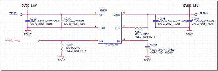
My customer consider using TPS22918-Q1 for SoC power sequencing at ADAS camera application and he asked us to provide the application schematic for 1.8V VIN and 0.5A Output load current. Would you please recommend the proper R and C external components for 1.8V/ 0.5A power rail in the typical application schematic as capture below?
Best regards,
DY
Hi DY,
Feel free to refer to the TPS22918 EVM for an example setup of the device: https://www.ti.com/lit/ug/slvuap0/slvuap0.pdf?ts=1617634445235&ref_url=https%253A%252F%252Fwww.ti.com%252Ftool%252FTPS22918EVM
The input and output capacitance is dictated by the strength of the supply and the output capacitance/filtering requirements. We use 1uF on the input and 0.1uF on the output. The external load resistance is system dependent. For the QOD resistance, this is determined by the customer's required turn off time. You can directly connect the VOUT to the pin for the fastest discharge. Finally, the CT capacitance is dependent on the required timing from the customer. We use a 1nF cap here but this can be higher or lower depending on the output capacitance and the allowed inrush current for the system.
Thanks,
Shreyas
Hi Shreyas,
Thanks for your kind response.
My customer made his application schematic of TPS22918-Q1 as attached below and he asked us to review if there is anything to be revised, especially capacitor rated voltage and resistor rated wattage also. My customer will use 0402(=1005) packages.
Best regards,
DY
Hi DY,
I believe the setup is correct as far as a standard setup goes. 0402 packages are acceptable.
Please note that according to the customer's real load and requirements, the CT capacitance can be increased or decreased.