This thread has been locked.

If you have a related question, please click the "Ask a related question" button in the top right corner. The newly created question will be automatically linked to this question.

BQ76952: Discharge MOSFET failing during short circuit event

Part Number: BQ76952

Hello,


We are facing problem while using BQ76952 to turn OFF MOSFETs during a short circuit event during discharge. The MOSFETs were initially ON at no load and suddenly a short circuit was created.


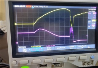
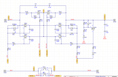
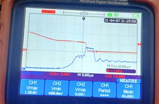
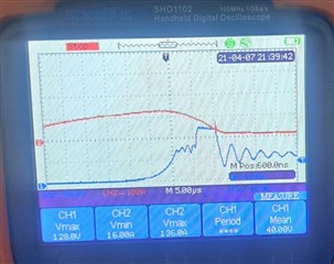
The schematic of the system is attached. We are using a Cgd value of 100pF on each of the 4 MOSFETs to remove oscillation faced at low loads during turn OFF. Please see the waveform of current during short-circuit and Vgs of Discharge FET. Only the discharge FET is failing, and nothing happens to charge FETs. Also, the SCD limit was 20A but the current went as high as 130A. Is this a response time issue? Please suggest how to correct the situation.

  • Hi Shyama,

    One of the features of the BQ76952 family is that you can set a short Protections:SCD:Delay so that the part can react while current may still be low so that the SCD current does not build to a high value which must be switched.  You might check that setting.  Even so the FET gate is held at about 11 V for a low RDSON and it takes time to discharge the gate to the threshold region where current actually drops. The rise in VGS at short circuit may be due to the BAT filter capacitor holding up the CP1, CHG and DSG voltages as the BAT+ and PACK+ drop due to the load, this can give even more voltage to discharge.  You might look at the voltage of D20 to see if it can be reduced to allow less rise of the voltage during SCD without causing a continuous load on the charge pump in normal conditions.  It looks like VGS goes from about 11 to perhaps 14V, so perhaps there is little improvement there.  You may not want D20 to be 18V since it would allow more rise.

    Cgd can be an effective way to suppress oscillations, it will also tend to resist turn off of the FET as the VDS  voltage starts to rise at turn off.  That may be good.

    The 2k individual gate resistors RG3 and RG4 seem large, one reference I have seen recommends these be about 10% of the total gate drive resistance.  I would expect these might be in the 10 to 200 ohm range but requirements will vary.  The remainder during turn off is R141 in parallel with R143, R144 which may look like 3 to 3.5k.  A ferrite bead may also be effective as RG3, RG4 to prevent oscillations having low DC resistance and high impedance at high frequency.

    The slow drop in VGS after the peak may be the DSG trying to turn off the FET.  DSG pulses toward LD, be sure LD is connected to PACK+ with 10k.  VGS will drop more slowly controlled by the resistance to the gate, so its smooth character is normal. Its slow drop indicates the total resistance to the gate is too large.  R143, R144 are likely set for the power dissipation during reverse charge so those won't change, again RG3 and RG4 should be smaller, R141 is the significant control on the turn off speed.  You want to get VGS to the threshold region quickly if possible, then your Cgd can help slow actual switching in the threshold region to avoid a large inductive spike from the cells. For this effect I would expect to see a Cgd to the common drive point rather than the individual, you might check recommendations of your design reference.

    There is an apparent oscillation when the current starts to drop quickly.  This might be oscillation of the FETs where they quickly trade the current back and forth heating each FET to failure.  After a period of this oscillation the FETs apparently fail.

    To summarize:

    • Make RG3 and RG4 smaller or a ferrite bead.  Perhaps 100 ohm if keeping the resistors
    • Check to see if Cgd is still effective for the no-current situation, check the design reference for guidance.
    • Make R141 smaller.  Too small and switching will be fast exciting the cell inductance, your FETs may go into avalanche or transients may overcome the input filters and break the IC inputs.  Too big and switching will be slow and the FETs may burn.  With small RGn you might try around 4k.
    • Suppress the turn off oscillation, again with individual beads or check your design reference on Cgd effect.
    • Iterate test as needed.  It is very frustrating when it breaks each test.
  • Hi,

    Thank you for your crystal clear inputs. We will re-test it while taking your inputs and update if we were able to resolve the issue.

  • Hello,

    We have currently moved the Cgd to the common drive point. We have reduced Rgn to 100 ohms. The MOSFET is now NOT failing, the Vgs waveform is also clean but the Vds spike seems to be large and unnatural. Please see the image below, one is Vgs and Vds and the other is Vds and I short circuit. Adding Cgd does slow down the rise time of Vds but the main spike seems to be coming just after the end of Miller plateau region or maybe just after Vgs crosses Vgs(th)

    Please suggest how to mitigate this. We are concerned if proper sizing/placement of decoupling capacitor is the problem. Also, we are not clear of the use of C34, 35, 36, 37 or how to effectively use it. We will reduce R141 after we solve this problem as we think these 2 problems might be decoupled.

    Vgs and Vds above

    Current and Vds above

  • Hi Shyama,

    The flat VDS at what looks like 130V might be a 100V FET going into avalanche at about 130% of rated voltage.  This is likely due to inductive response of the system, V = L x dI/dt.  Cell voltage will rise, load loop voltage will fall, the FET is between them. Your resistances to the driver should control most of the turn off speed, Cgd will slow it some if used.  Your current does not look like a really steep drop but you will understand better than I. 

    You might look at the voltage of PACK+ and BAT+ at turn off.  BAT+ will peak at turn off due to the L x dI/dt.  PACK+ may be driven negative if your load loop is large (SCD wire). If PACK+ goes sufficiently negative Q20 can turn on causing the remainder of turn off to happen very quickly.  Fast turn off means short dt and large V.  Q20 does not normally have a drain resistor to the power FET gate point because it is a clamp transistor to keep a voltage that is already 0 at 0.  If it is turning off the FET in your system due to inductances you may want a resistance to slow the turnoff caused by Q20 during transient.  As a clamp some drain resistance is ok as long as it does not form a sufficient divider with  R143, R144 to turn on the power FET again in the reverse charger/voltage condition.

    C34, 35, 36, 37 are ESD capacitors.  They carry a high speed & current ESD pulse short across the PACK terminals and across the FETs to the cells.  Two are used in series so that it takes a double fault to short the pack or bypass the FETs.  They are probably too small to be an effective snubber for an SCD transient.  They do have a side effect of waking the IC on cell connection since the divider effect raises the PACK+ and LD pin voltage to about 1/2 the step applied to BAT+.

    It seems you are now on  your way to optimizing your circuit.