This thread has been locked.

If you have a related question, please click the "Ask a related question" button in the top right corner. The newly created question will be automatically linked to this question.

TPS63810: TPS63810 question

Part Number: TPS63810

HI team,

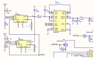
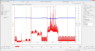
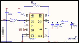
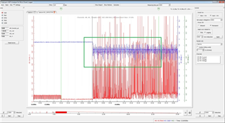
sometimes, at sharp load changes chip falls to abnormal state, unable to maintain stable output voltage, output generates spikes. And chip will retain this state permanently, initialization/refreshing voltage settings through I2C returns chip back to normal operation. Is there a solution to prevent chip from switching to this abnormal state?

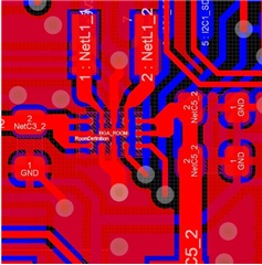
I've provided snippets of chip wiring and two cases of behaviour.

Thank you very much.

Best regards,

  • Hi, Zhonghui,

    what do the red and blue line stand for?

  • Hi Jasper,

    Hi, sorry for late reaction . Red line is current at load and blue line is voltage . I not sure about place where was voltage connected. Most relevant is red it's current at load behind TPS.
    Also we have stumbled at another problem. Sometimes short circuit protection doesnt work in TPS, sometimes it burns out after short. Overall schematic is complex, but at output there is MOSFET and 0.1 Ohm shunt (at minimal) serially with SHORT CIRCUIT. Please, look at input configuration. Two switches with fixed limits 0.5 and 1.5 А. Short circuit behavior is way worse with Vbat branch. There is impression that short circuit happens in internals of TPS too. The more current capacity at in the input the more fatal cases. We have changed L2 to 0.25 Ohm and this cures the problem but we are barely meet output specification as 1A. P.S. About voltage line - it is voltage at load.

    Best regards,

  • Hi Zhonghui,

    the device should be able to protect itself at short protection condition. could you check if the layout is the same as suggested in datasheet?

    the input capacitor and output capacitor loop are the most importance.

  • Hi Jasper,

    we are continuimg to burn chips. It seems, worst case is 2.5 Ohm load (90% guarantee of burn fault), I dont know why, maybe this problem related to other mechanism in chip that goes wrong. There is difference between pictures 'wrong' and 'right'. Load(DUT) voltage is set around 3.7 V. When all goes right voltage just slightly drops at heavy load, and for wrong case voltage defaults to 3.3V (chip catch reset). But this reset state is wrong, chip cannot maintain load current even small one. Once voltage settings is refreshed by I2C - it comes back to life and behaves normally. Added picture of our routing. 2-layer board, not exact with reference.

    Thanks

    Best regards,

  • Hi Zhonghui,

    do you mean the IC is damaged? could you share the layout image again?

    maybe we can discuss this through email.

  • Hi Jasper,

    Sorry, I'll send you the picture.

    Thanks

    Best regards,

  • Hi Zhonghui,

    the layout is not good. the output capacitor loop is long. 

    which pin is damaged? also please apply an EVM for reference