Dear TI Team,
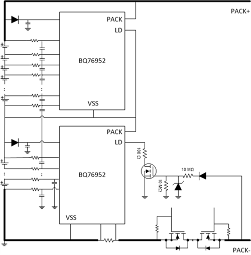
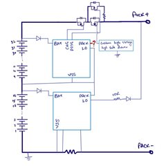
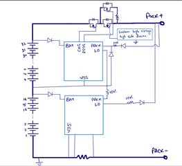
I am trying to stack two bq76952 together for a 32S BMS design with following design considerations:
- Upper IC will be operating with VSS referenced to the top of 16th cells
- SRP and SRN of the top IC will be shorted
- Upper IC will drive the high side DFET, CFET and PDSGFET of the combined battery pack
- DDSG and DCHG signals from lower IC will feed the DFETOFF and CFETOFF input of upper IC through isolators for communicating faults
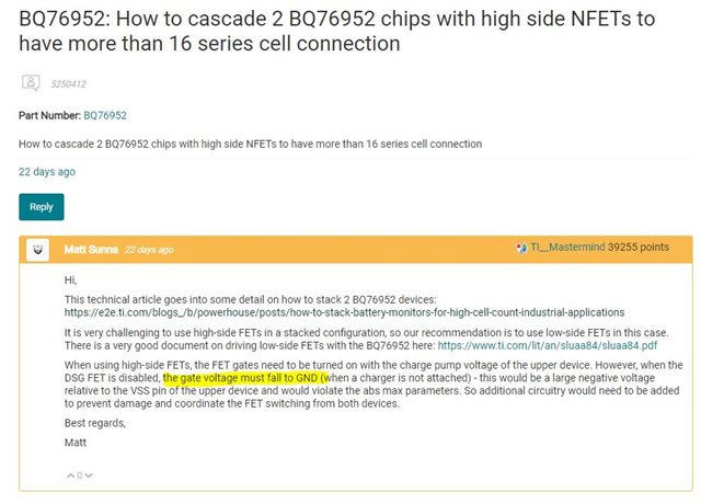
However in one of the posts it is mentioned (as in the screenshot below) that gate voltage must fall to GND for proper operation of high side MOSFETs. Can it be possible that the gate voltage of high side MOSFETs falls to VSS of the upper IC (i.e. top of 16th cell) for safe turn ON and OFF of the MOSFETs. As per my understanding, zero VGS voltage must be enough to turn OFF the high side MOSFETs.
Thanks and Regards
Manuj Agrawal