


Other Parts Discussed in Thread: LM5146, , LM5146-Q1
I posted an issue previously and was talking with Tim Heggarty
I have a CE issue on the telecoms port and have no issue with my input power port.
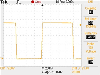
I've been in the lab and see no ringing on the switching node that is discernible using short earth on my 150MHz Tek scope. I get a clean 550kHz trace.
I'm getting a peak at 555kHz at 15.7dB above the limit at 89.7dBuV (Average), and at 1.107MHz, 0.77dB below at 73.23dBuV, and the other harmonics fall away.
I'm trying to understand how it's coupling onto the telecomms port and how to solve this.
I don't want to change the layout yet, and want to explore other options on existing design.
Option 1: Add snubber to switching node at 2.2 ohms and 220pF as suggested on previous thread
Option 2: Increase BST resistor, to slow SW edge, not sure what value I can use to avoid messing with regulation stability.
Option 3: Since I'm not using screened cables for my network ports. Remove 2kV capacitors between ETH_GND and system GND. The GND plane may be the coupling mechanism.
In the past I used to keep my design on one layer and void under the switching node, but followed the LM5145 layout example almost exactly. Wish I'd seen LM5146 layout before, it's all on one layer.
Any advice appreciated.

