Other Parts Discussed in Thread: MSP430FR2155,
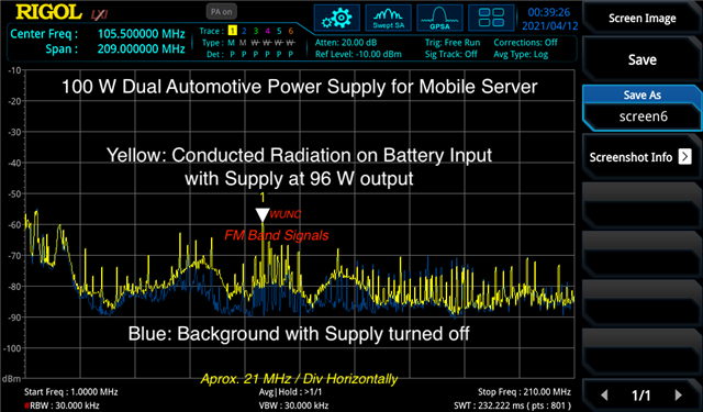
I've got a nifty two supply PCB for powering servers in a vehicle environment up and running. Each supply provides about 50 W of power with battery input voltages from 8 to 18V, and can keep the output stable for brief periods (a few seconds, mostly a thermal concern) for inputs as low as 6V. As such, the server stays up even if the vehicle is being cranked. A small uP, MSP430FR2155, monitors voltages, currents and ambient temperature in addition to booting the server and taking it down after ignition goes away or if the battery voltage is too low or if the ambient temperature gets out of range. It uses the I2C to set the output voltages of the two supplies, does a "black box" log of currents and faults seen while the supply is running. A serial port is used to configure and view logs. A 2nd serial port talks to the server to advise on battery conditions and when the server needs to take the system down because the supplies need to be turned off. Gratuitous annotated PCB pix included, this is a "What you can do with TI chips" poster child.
I am having difficulty understanding the role of the OCP setting in R3 of the registers. From the data sheet, this field "Sets the response time of the device when the output overcurrent limit is reached." As I understand it, there are two current limits in play on this chip. One is the current limit set via Register 2 (in conjunction with the current sense resistor which in my case is a 10 mOhm resistor). The other is an internal current source to protect the on board FETs set at about 16 amps. So my questions are:
1) Does the POCP_DELAY use the overcurrent status from the Register 2 setting, the 16 amp internal "safety" current sense, or both?
2) Exactly what happens after the configured "response time" ? Does this affect the power supply output by the voltage dropping to insure that the specified maximum current is not exceeded ? Does this determine when the OCP bit in the Register 7 "Status" is set ? Both ?
3) Is it a correct assumption that the goal here is to allow the part to output a current in excess of the Register 2 setting for a period of time (with the 16 amp "safety" inductor current limit always in effect) before the part drops the voltage. This would be a mechanism to accommodate a step increase in load scenario where the supply was stable at some output voltage and then a load, possibly with a large inrush current due to capacitors, was applied ?
In addition to the gratuitous PCB pix, enclosed is a pix of the input voltage (top, yellow) and output voltage (bottom, green) of the supply (output voltage = 12V) in response to connecting and disconnecting a 4 amp load. Very reasonable changes in voltages, the regulation is pretty much as good as it gets. However if I have the R3 set to 128uS, I see the OCP bit set in R7 under this test condition. I've not tried other settings as I don't want to stress the chip if I don't understand exactly what is going on.

![]()