Other Parts Discussed in Thread: LM5145, LM25149-Q1, CSD18533Q5A, LM5146-Q1
Hello,
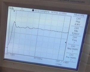
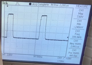
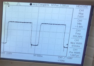
I designed controller and cannot get it to pass EMC. I have tried adding ferrits to input and output wires, changing CBoot, and adjusting values of the snubber capacitor and resistor. I am out of ideas of what else to try. I realize now that the vias in the SW Node need to be removed and the trace needs to run on the top layer. Scraping the copper off the bottom layer and cutting the bottom trace and replacing it with a wire on the top layer did not make a difference. I have also added smaller caps to decouple the input and output caps of the regulator with no affect. There is ringing in the switch node that I am not able to suppress further. I have shutdown all other subsystems on the PCB so the noise is coming from this part. Please let me know if you require additional information. Thank you for any assistance you can provide.
Controller Parameters:
Vin 40V
Vout Max 9.25V
Current limit 8.5A
This controller runs mostly in current limited mode.
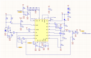
Schematic
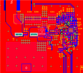
Top Layer

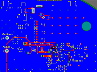
Bottom Layer
Stackup

Switchnode (Probe 10X)
High side gate to source
Low side gate to source
EMC test report