A related question is a question created from another question. When the related question is created, it will be automatically linked to the original question.
If you have a related question, please click the "Ask a related question" button in the top right corner. The newly created question will be automatically linked to this question.
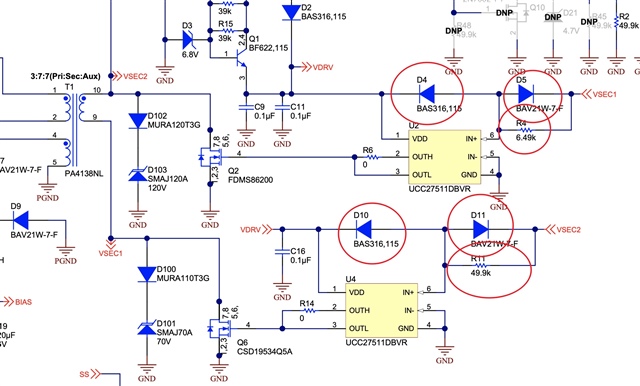
UCC2897A: PMP10861 the gate driver circuit UCC27511
In PMP10861 reference design schematic, UCC27511 low side gate driver is used. What's the purpose of these components? How to calculate the resistor value?
When VSEC goes HIGH during initial start up, SR body diodes are used for start-up, VDRV is not yet present, U2-IN+ is connected to U2-VDD through D4 which gets U2 started until VDRV takes over and provides bias to U2 and U4. This is how D4 and D10 are used for starting up the SR drivers. R4 is used to slow the U2-IN+ rising edge but the U2-IN+ falling edge bypasses R4 through D5. This technique is commonly used at the input to a gate driver when a turn on delay needs to be introduced. The value of R4 (R11) is adjusted during bench testing to match the secondary SR timing compared to the primary.
For PMP10861 where 3:7 turn ratio of the transformer, the secondary winding voltage (VSEC1/VSEC2) will be very high especially at 36Vin, means the U2-IN+ or U4-IN+ will be applied with high voltage (VSEC through R4/R11), however datasheet of UCC27511 only allows-0.3V to +20V, any risk to run at much high voltage level on IN+ pin?
per my calculation, with 3:7 ratio, at 36Vin, the SEC2 max is 84V, at 9Vin, SEC1 max is 28V, both of them are above the UCC27511 spec.