A related question is a question created from another question. When the related question is created, it will be automatically linked to the original question.
If you have a related question, please click the "Ask a related question" button in the top right corner. The newly created question will be automatically linked to this question.
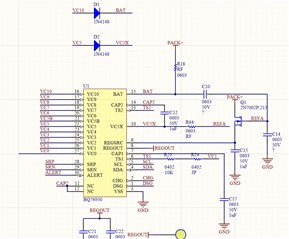
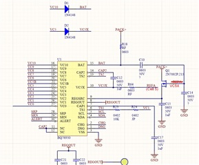
In the BQ76930 data sheet these components are called Rf and Cf, there is a range shown but it includes the BQ76920 also. Generally with the BQ76930 or BQ76940 Rf and Cf are 1k ohm and 10 uF. The values are large and used with large Rc resistors (1k) to avoid depleting the power filter during short circuit timing, see the application note https://www.ti.com/lit/pdf/slua749 for more information if desired.
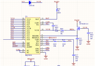
For proper operation TS2 needs a pull down to VC5X, normally a thermistor or similar resistor. TS1 also needs a pull down to VSS and a rising edge for boot. A constant high does not provide a boot or prevent shutdown.
In the schematic segment the Cf capacitors C10 and C14 should go to VC5X and the Rf would come from the cell 5 to VC5X. I have marked this on the diagram below. Some designers will place a resistor to the Q1 gate and one in the Q1 drain to help with ESD and reduce power dissipation in Q1. There is a section in the application note above on REGSRC if it is helpful.
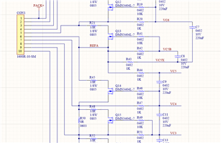
1. Yes, cell 5 should go to 3 filter resistors, 1 for VC5, 1 for VC5X, 1 for VC5B as you show. It will also connect to to the cell 5 cell balance resistor and the cell 6 N-ch FET as you show.
2. Almost.
C12 is the (Ccap in data sheet) CAP2 filter capacitor, it should stay 1 uF
C14 appears to be the Cf VC5X power filter capacitor, it should typically be 10 uF.
R64 seems to be the Rf filter resistor for VC5X, but that is already shown in the other schematic clip as R43. Delete R64.
R18 is typically 1k, yes.
C10 from the first schematic is/was Cf for the BAT pin, it should be retained, 10 uF typical.
Some designers prefer resistors in the gate and drain paths of Q1. If interested see the REGSRC section of the application note www.ti.com/lit/slua749
I'm not sure of the options you have available. If you click on my username you may have an option to send me a private message, or request friendship and we can have a private message exchange. I will look for your message.